In high-speed PCB design, the return path is not an afterthought—it is the foundation of signal integrity. A poorly designed return path creates ground loops, increases electromagnetic interference (EMI), and degrades signal quality. For B2B engineers designing high-speed PCBs for export, ensuring a continuous, low-impedance return path is critical. This Pillar Content provides a definitive guide to setting up return path design checks in the three most popular EDA tools: Altium Designer, Cadence Allegro, and KiCad. By adopting these checks, you can prevent costly board spins and ensure your design meets the rigorous demands of high-speed applications.
Why Return Path Checks Are Essential for High-Speed PCBs
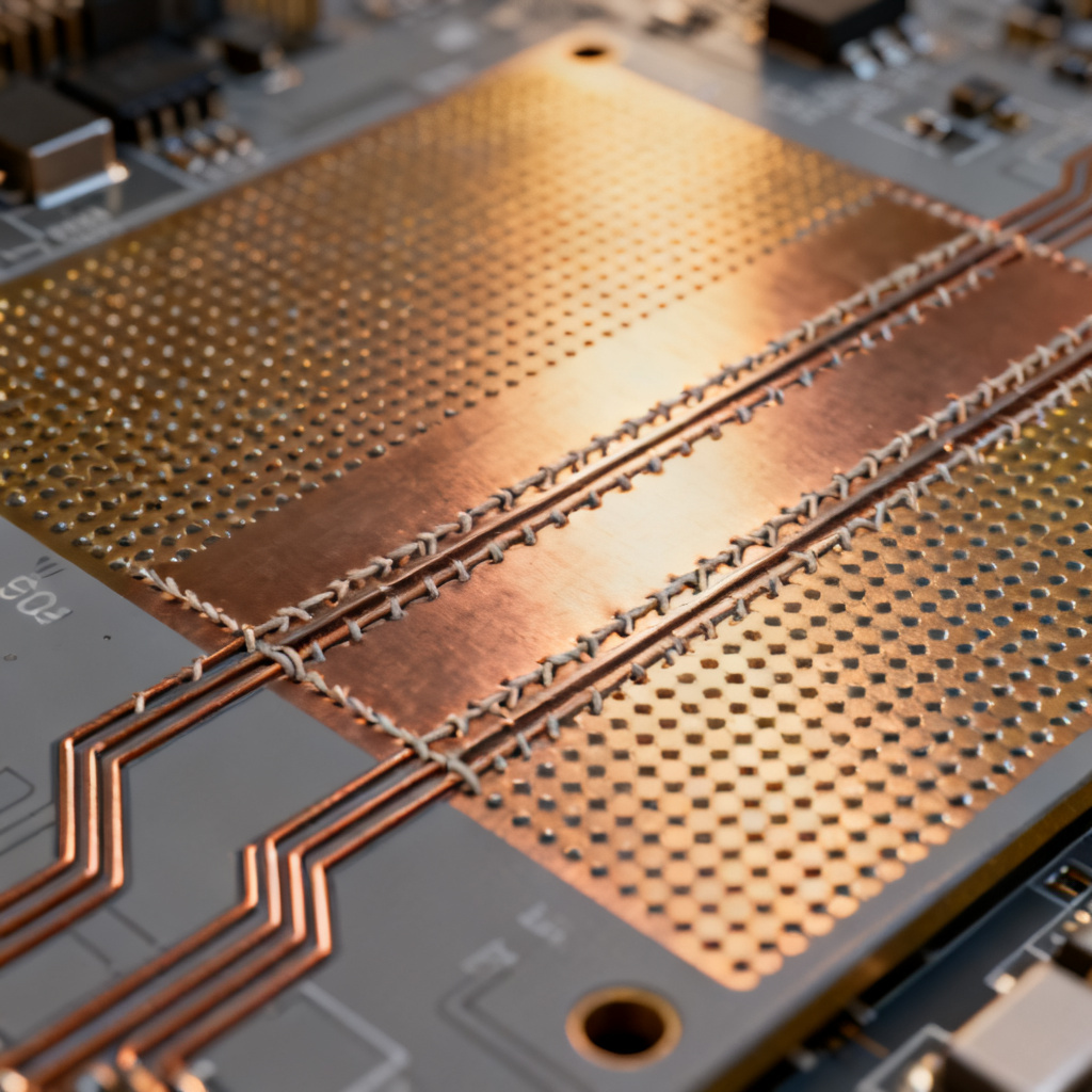
Before diving into tool-specific setups, understand the physics. Every signal trace is part of a transmission line. The signal current flows out on the trace, and the return current flows back through the nearest reference plane (usually ground or power). At high frequencies (above 1 GHz or even lower for fast edge rates), the return current concentrates directly under the trace due to skin effect and proximity effect. Any break in this path—such as a split in the ground plane, a missing via, or a void—forces the return current to detour, creating a large loop area. This loop radiates EMI and introduces inductance, degrading signal integrity.
Key failure modes to check:
- Split reference planes (e.g., analog/digital splits).
- Missing stitching vias near layer transitions.
- Voids under critical traces (e.g., via antipads or cutouts).
- Poor via placement for differential pairs.
- Unreferenced traces crossing slot gaps.
Now, let’s configure automated checks in your EDA tool to catch these issues early.
Setting Up Return Path Checks in Altium Designer
Altium Designer offers powerful rules and scripting tools to enforce return path integrity. The primary methods are using the Design Rule Check (DRC) engine and the PCB Rules Editor.
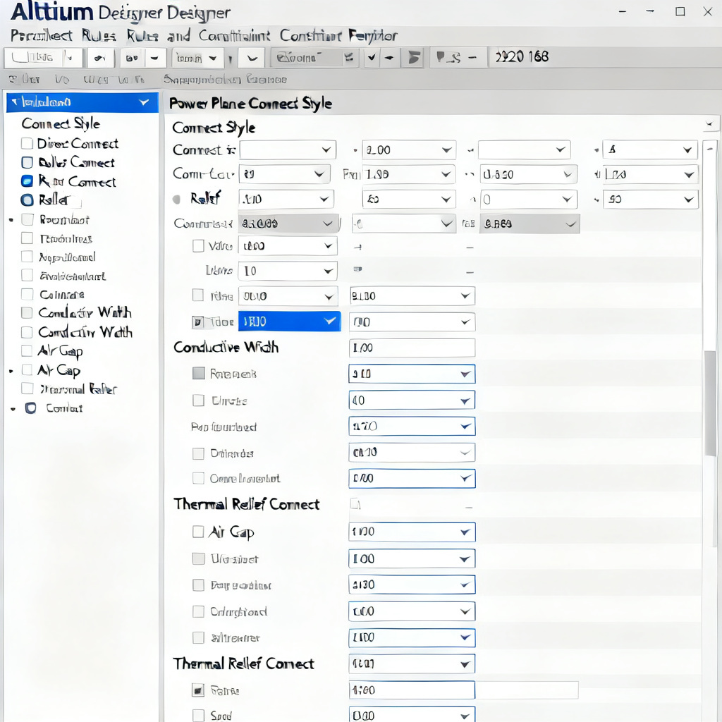
Enable Plane Connectivity Rules
Step: Open the PCB Rules and Constraints Editor (Design > Rules). Rule: Navigate to Plane > Power Plane Connect Style. Setting: For high-speed signals, use a Direct Connect style for all vias and pads connected to ground planes. This minimizes inductance. Alternatively, use a Relief Connect with a minimum of 4 spokes for thermal management but ensure the spoke width is at least 10 mils for low impedance. Check: Run a DRC (Tools > Design Rule Check). The rule flags any via or pad that has insufficient connection to the plane.
Implement the “UnRouted Net” Rule for Via Stitching
Step: In the same rules editor, go to Routing > UnRouted Net. Rule: Create a custom rule for a net class named GND_STITCHING. Assign all ground vias to this class. Set the rule to check for Net Topology—ensure every ground via connects to the same plane without floating segments. Check: This catches missing stitching vias near high-speed trace layer changes. For example, if a signal on Layer 1 switches to Layer 3, the DRC will flag any ground via that is not within 100 mils of the transition.
Use the “Room Definition” for Plane Cutout Detection
Step: Go to Design > Rooms > Define Room from Selected Objects. Rule: Create a room around a high-speed differential pair or clock trace. Then, in the rules editor, add a Clearance rule between the room and any plane cutout (using the polygon cutout layer). Check: The DRC will warn if a plane void (e.g., from a via antipad) encroaches within the room, indicating a broken return path.
Script-Based Return Path Analysis (Advanced)
For comprehensive checks, use Altium’s Scripting System (DelphiScript or Python). A custom script can: Quantify loop area: Calculate the area between a signal trace and its nearest reference plane. Flag via spacing: Check that stitching vias are placed at intervals less than 1/20th of the wavelength of the highest harmonic. Implementation: Download the “Return Path Analyzer” script from the Altium Community. Run it via Tools > Scripts > Run Script. The script outputs a list of violations with coordinates.
Visual Inspection with 3D View
Step: Switch to 3D view (View > 3D Layout Mode) and enable transparency for planes. Check: Look for any trace that crosses a visible gap in the ground plane. Use the Measure Distance tool to verify clearance.
Setting Up Return Path Checks in Cadence Allegro
Cadence Allegro is the industry standard for complex, high-speed designs. Its constraint manager is the most granular for return path analysis.
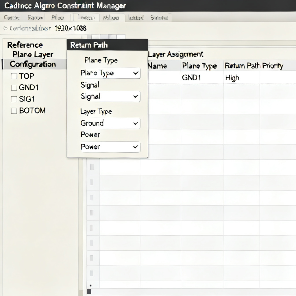
Define Return Path Constraints in the Constraint Manager
Step: Open Constraint Manager > Electrical > Signal Integrity > Return Path. Rule: For each net class (e.g., DDR_CLOCK), set the Return Path Type to Reference Plane. Specify the Reference Plane Layer (e.g., GND layer 2). Check: Allegro will automatically flag any net that crosses a plane split or changes reference planes without a stitching via.
Use “Plane Void Check” Rule
Step: In Constraint Manager > Physical > Plane, enable Plane Void Check. Setting: Set a Minimum Void Clearance of 10 mils for any trace to the edge of a plane void (e.g., via antipad). Check: Run a DRC (Setup > Constraints > DRC). This catches cases where a via antipad is too close to a high-speed trace, effectively creating a gap in the return path.
Implement Via Stitching Checks via “Net Topology”
Step: In Constraint Manager > Electrical > Topology, create a topology template for high-speed nets. Rule: Add a Stitching Via constraint. Set the Maximum Via Spacing to 1/10th of the wavelength (e.g., 100 mils for 5 GHz signals). Check: Allegro’s topology checker will highlight any net that lacks a stitching via within the specified distance from a signal via.
Use the “Return Path Analyzer” (SKILL Script)
Cadence provides a built-in SKILL script for deeper analysis. Step: In the command window, type skill and then load("return_path_analyzer.il"). Function: It computes the return path impedance for each net. A value above 1 ohm indicates a poor return path. Check: Run the script and review the output log. It lists nets with high impedance, often caused by plane splits or missing vias.
Differential Pair Return Path Checks
Step: In Constraint Manager > Electrical > Differential Pair, enable Return Path Symmetry. Rule: Set Maximum Phase Imbalance to 5 degrees. A poor return path causes imbalance. Check: Run DRC. If the ground plane under one trace is broken, the phase imbalance will exceed the limit, flagging the pair.
Visual Verification with “Plane Viewer”
Step: Use Display > Plane Viewer to see the copper distribution on each layer. Check: Overlay the high-speed net layer with the plane layer. Look for any trace that lies over a gap (e.g., a split between analog and digital ground). Use the Measure tool to confirm clearance.
Setting Up Return Path Checks in KiCad
KiCad, while open-source, is increasingly capable for high-speed design. Its rule system and plugin ecosystem allow robust return path checks.
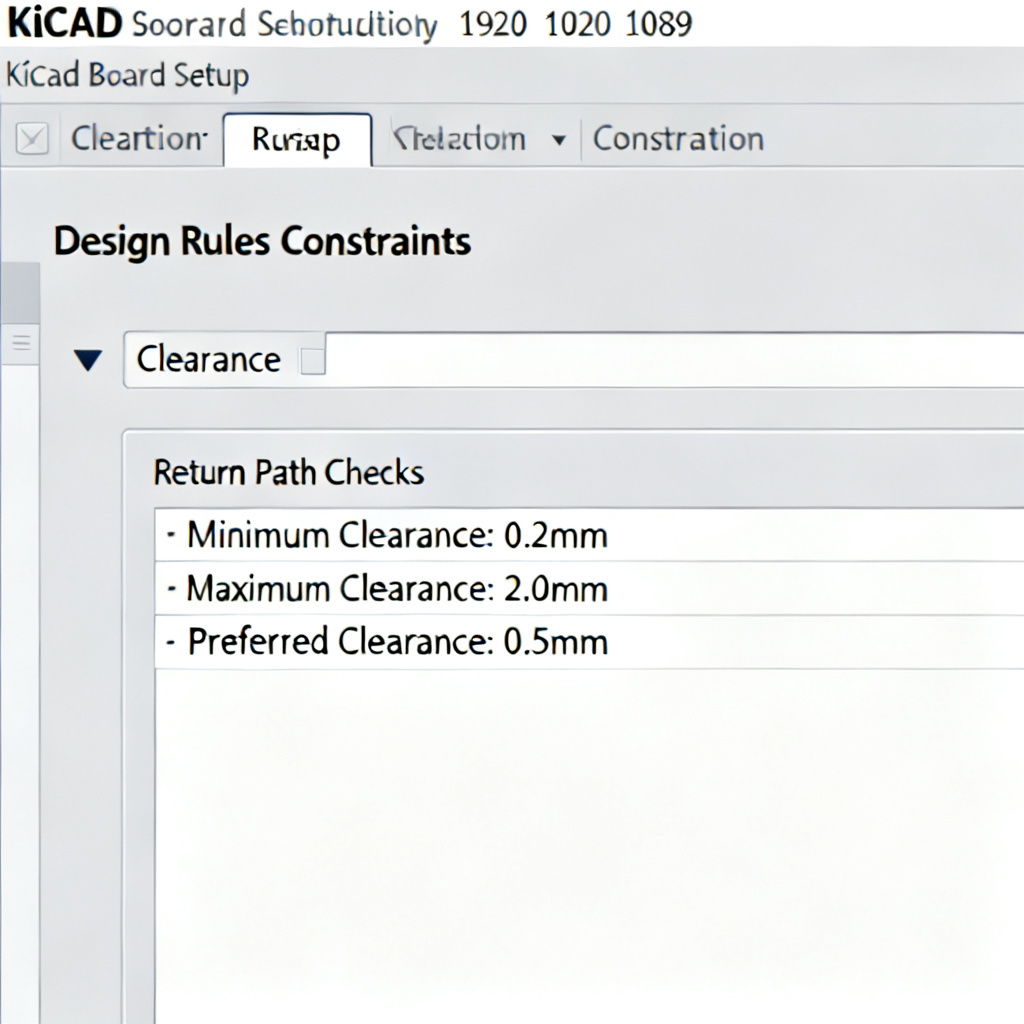
Use the “Design Rules” for Clearance and Plane Checks
Step: Go to File > Board Setup > Design Rules > Constraints. Rule: Set Clearance to 10 mils for all net classes. This is a basic but critical check. Check: Run DRC (Inspect > Design Rules Checker). It flags any trace that is too close to a plane cutout or via antipad.
Implement the “Zone to Zone Clearance” Rule
Step: In the same design rules, go to Constraints > Zone to Zone Clearance. Rule: Set a minimum clearance of 20 mils between two different ground zones (e.g., analog and digital ground). This prevents accidental splits. Check: DRC will warn if the gap is too narrow, which could cause return current crowding.
Use the “Plot” Function for Visual Plane Analysis
Step: After routing, go to File > Plot. In the plot dialog, select F.Cu and GND layer (e.g., B.Cu). Check: Export the gerber files. Overlay the signal layer and the ground plane layer in a Gerber viewer (e.g., Gerbv). Look for traces that cross gaps in the plane. This is a manual but effective check.
Use the “KiCad Return Path Plugin” (Third-Party)
Step: Install the plugin from the KiCad Plugin Manager (search for “Return Path Checker” or “Via Stitching Analyzer”). Function: This plugin scans all nets and identifies: Nets that cross plane splits; Nets with missing stitching vias near layer transitions; Nets with high loop area. Check: Run the plugin via Tools > External Plugins > Return Path Checker. It generates a report listing all violations with coordinates.
Manual Via Stitching with “Via Stitching” Tool
Step: Select a ground net, then use Tools > Via Stitching. Set the Stitching Pattern to a grid with 100 mil spacing. Check: After stitching, run DRC to ensure no ground vias are floating (check the “Unconnected Items” rule).
Use “Net Inspector” for Reference Plane Verification
Step: Go to Inspect > Net Inspector. Select a high-speed net (e.g., CLK). Check: In the net properties, look for Reference Plane field. KiCad does not automatically assign this, but you can manually verify by viewing the 3D viewer (View > 3D Viewer) and checking if the trace is over a solid copper pour.
Best Practices for Return Path Checks Across All Tools
Regardless of your EDA tool, follow these universal best practices:
- Use a Solid Ground Plane: Never split ground planes under high-speed traces. If you must split (e.g., for isolation), place a bridge or use a differential pair with a common-mode choke.
- Stitching Vias at Layer Transitions: Place a ground via within 100 mils of every signal via that changes layers. For differential pairs, place two vias (one for each trace) symmetrically.
- Avoid Voids Under Critical Traces: Check that via antipads (holes in the plane for via barrels) are not directly under high-speed traces. Use a clearance of at least 10 mils.
- Check Return Path for Power Planes: If a signal references a power plane (e.g., 3.3V), ensure there is a decoupling capacitor near the source and load to provide a low-impedance return path to ground.
- Use Automated Scripts: For large designs, manual checking is impossible. Invest time in setting up DRC rules or using scripts (Altium Scripts, Cadence SKILL, KiCad Plugins) to automate return path analysis.
FAQ: Return Path PCB Design Checks
What is a return path in high-speed PCB design?
How do I check return path violations in Altium Designer?
Can KiCad perform automated return path design checks?
Why is via stitching important for return path integrity?
What tools are available for return path analysis in Cadence Allegro?
Return Path Checks Comparison Table
| EDA Tool | Return Path Check Feature | Key Setting |
|---|---|---|
| Altium Designer | Power Plane Connect Style | Direct Connect for low impedance |
| Altium Designer | UnRouted Net Rule | Net class GND_STITCHING |
| Altium Designer | Room Definition for cutout | Clearance rule with polygon cutout |
| Cadence Allegro | Constraint Manager Return Path | Reference Plane Layer assignment |
| Cadence Allegro | Plane Void Check | Minimum Void Clearance 10 mils |
| Cadence Allegro | Net Topology Stitching Via | Maximum Via Spacing 100 mils |
| KiCad | Design Rules Clearance | Clearance 10 mils |
| KiCad | Zone to Zone Clearance | Minimum 20 mils between zones |
| KiCad | Return Path Plugin | Scans for plane splits and missing vias |
Conclusion
Setting up return path design checks in your EDA tool is not optional for high-speed PCB success. By implementing the rules and scripts described above in Altium Designer, Cadence Allegro, and KiCad, you can detect and fix return path violations before fabrication. This ensures your high-speed PCBs maintain signal integrity, minimize EMI, and pass first-pass validation—critical for B2B export success.
For further reading, explore our guides on High-Speed PCB Stackup Design and Via Optimization for Signal Integrity. If you need a custom return path analysis script for your specific EDA tool, contact our engineering team for a consultation.