Crosstalk in high-speed PCB design is the electromagnetic coupling of energy from one signal trace onto an adjacent trace. Mastering crosstalk in high-speed PCB is essential for reliable data transmission. This comprehensive guide explains NEXT vs FEXT, the 3W rule, six proven methods to reduce crosstalk, and differential pair crosstalk considerations. Part of our Signal Integrity Guide.

Table of Contents
What Is Crosstalk in High-Speed PCB Design?
Crosstalk in high-speed PCB design refers to the electromagnetic coupling of energy from one signal trace onto an adjacent trace. When a signal travels on a PCB trace, it creates electric and magnetic fields. If another trace lies nearby, it unintentionally captures some of that energy. Understanding crosstalk in high-speed PCB is the first step toward building robust digital systems.
Think of it like two cars driving close together on a narrow road. When one swerves, the other feels the disturbance. Similarly, when an “aggressor” signal switches, the nearby “victim” trace experiences unwanted voltage fluctuations. Crosstalk in high-speed PCB can cause data errors, timing jitter, and increased EMI.
Excessive crosstalk in high-speed PCB leads to:
- Data errors from false switching
- Timing jitter and shift that degrades margins
- Increased EMI (electromagnetic interference)
For broader signal integrity context, including impedance matching and return path design, visit our comprehensive Signal Integrity Guide.
NEXT vs FEXT: Key Differences in PCB Crosstalk
When analyzing crosstalk in high-speed PCB designs, depending on where you measure the victim line, you will see two distinct types: near-end crosstalk (NEXT) and far-end crosstalk (FEXT). Each type behaves differently and requires different mitigation strategies.
Near-End Crosstalk (NEXT)
| Property | Description |
|---|---|
| Definition | Interference measured at the source end (near the driver) |
| Travel direction | Opposite to the aggressor signal (backward) |
| Coupling | Capacitive + inductive (add constructively) |
| Amplitude | Large; saturates after a certain trace length |
Far-End Crosstalk (FEXT)
| Property | Description |
|---|---|
| Definition | Interference measured at the receiving end (near the receiver) |
| Travel direction | Same direction as the aggressor (forward) |
| Coupling | Capacitive + inductive (partially cancel) |
| Amplitude | Smaller than NEXT; grows with trace length |
| Characteristic | NEXT | FEXT |
|---|---|---|
| Measurement end | Near driver | Near receiver |
| Travel direction | Backward | Forward |
| Length dependence | Saturates | Increases with length |
How Crosstalk Occurs: Coupling Mechanisms
Crosstalk in high-speed PCB arises from two fundamental coupling mechanisms rooted in Maxwell’s equations. Both mechanisms contribute differently to NEXT and FEXT.
| Coupling Type | Principle | Main Contribution |
|---|---|---|
| Capacitive | Electric field through parasitic capacitance | Contributes to both NEXT and FEXT |
| Inductive | Magnetic field through mutual inductance | Dominant contributor to NEXT |
Factors That Influence Crosstalk Severity
Several physical parameters directly affect how much crosstalk in high-speed PCB your design will experience. The table below summarizes key factors.
| Factor | Trend |
|---|---|
| Spacing (S) | Larger → Lower crosstalk |
| Parallel length (L) | Longer → Higher crosstalk |
| Trace width (W) | Wider → Higher crosstalk |
| Dielectric thickness (H) | Thicker → Lower crosstalk |
| Signal rise time | Faster → Worse crosstalk |
| Reference plane integrity | Broken → Increased crosstalk |
Critical rule: Never route signals over splits in their reference planes. The return current cannot jump across the gap, creating larger loop areas that dramatically increase inductive crosstalk in high-speed PCB. See our Return Path Design Guide for detailed guidance on reference plane continuity.
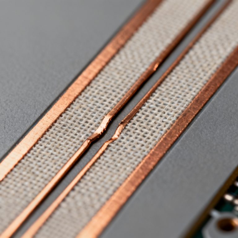
The 3W Rule for Crosstalk Reduction
The 3W rule is the most widely used and effective guideline for crosstalk in high-speed PCB reduction across the industry. Following this simple rule can reduce crosstalk by 80-90%.
What Is the 3W Rule? Center-to-center spacing ≥ 3 × trace width. When you apply the 3W rule to reduce crosstalk in high-speed PCB, you create enough distance between traces to minimize field coupling. Example: If trace width = 5 mils, center-to-center spacing must be ≥ 15 mils (air gap = 10 mils).
When Stricter Rules Are Required
| Scenario | Recommended Spacing |
|---|---|
| Clock lines adjacent to signals | ≥ 4W |
| Between differential pairs | ≥ 4W |
| High-speed near sensitive analog | ≥ 5W |
| Outer layer (microstrip) | Larger than 3W |
| 25 Gbps+ SerDes | ≥ 5W |
6 Proven Methods to Reduce Crosstalk in High-Speed PCB
Here are six practical techniques to minimize crosstalk in high-speed PCB designs. Use them in combination for best results.
Method 1: Increase Spacing
Effectiveness: The single most effective method to reduce crosstalk in high-speed PCB. Doubling spacing reduces crosstalk by about 50-75%.
Method 2: Use Stripline (Inner Layer)
Effectiveness: Moving signals to inner layers dramatically reduces crosstalk in high-speed PCB because dual reference planes contain electromagnetic fields.
| Trace Type | Crosstalk Level | Reason |
|---|---|---|
| Microstrip (outer) | Higher | Only one reference plane |
| Stripline (inner) | Lower | Dual reference planes contain fields |
Method 3: Add Guard Traces with Vias
Effectiveness: A grounded trace between aggressor and victim can further reduce crosstalk in high-speed PCB. Critical rule: Must be stitched to ground with vias every 100 mils maximum. Without vias, a guard trace makes crosstalk worse.
Method 4: Reduce Parallel Run Length
Effectiveness: Crosstalk in high-speed PCB integrates along the entire parallel length. Keep parallel runs shorter than the rise time distance (e.g., < 1.2 inches for 200 ps rise time on FR4).
Method 5: Route Adjacent Layers Orthogonally
Effectiveness: Route horizontal on one layer, vertical on the adjacent layer. Never route two high-speed signals directly on top of each other, as this creates vertical crosstalk in high-speed PCB.
Method 6: Choose Low-Dk Materials
Effectiveness: Lower dielectric constant spreads fields more, reducing coupling. Higher cost; justified for >10 Gbps designs where crosstalk in high-speed PCB becomes extremely critical.
| Material | Dk | Relative Crosstalk |
|---|---|---|
| Standard FR4 | 4.2-4.5 | Baseline |
| Mid-loss | 3.8-4.2 | ~10% lower |
| Low-loss (Rogers) | 3.4-3.7 | ~30% lower |
Crosstalk in Differential Pairs
Differential pair crosstalk behaves differently than single-ended. Differential pairs have inherent immunity because common-mode noise is rejected by the receiver (typically 20-30 dB better than single-ended). However, crosstalk in high-speed PCB can still affect differential pairs if not properly managed.
| Requirement | Value |
|---|---|
| Within-pair spacing | S ≤ 2W (tight coupling) |
| Between different pairs (same layer) | ≥ 4W or 20 mils |
| Between differential and single-ended | ≥ 4W |
| Pairs on adjacent layers | Route orthogonally |
Common mistake: Keeping within-pair spacing tight while placing different pairs too close. The 3W/4W rule applies between pairs, not within a pair. For complete differential pair routing guidelines including length matching and impedance control, see our Differential Pair Routing Guide.
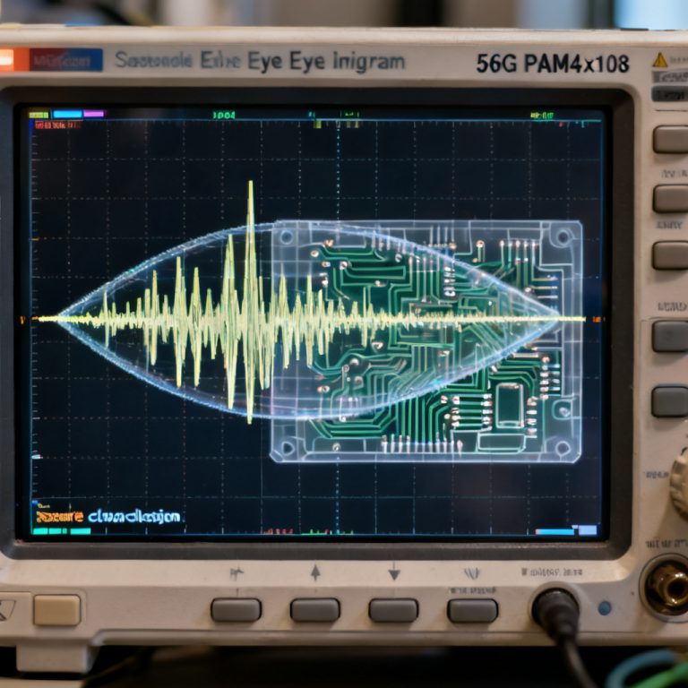
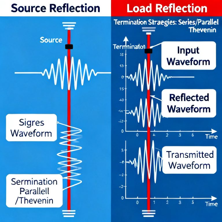
Simulation and Measurement of Crosstalk
Crosstalk simulation is essential for verifying your design before fabrication. Without simulation, crosstalk in high-speed PCB may go undetected until hardware testing. Crosstalk acceptance criteria vary by interface type.
Simulation Tools
| Tool | Application |
|---|---|
| HyperLynx (Siemens) | Pre and post-layout analysis |
| Allegro Sigrity (Cadence) | Post-layout extraction |
| ADS (Keysight) | High-precision EM simulation |
Measurement Methods
| Tool | Purpose |
|---|---|
| Oscilloscope | Measure NEXT/FEXT directly |
| TDR | Locate coupling points |
| VNA | Measure S-parameters (S31=NEXT, S41=FEXT) |
Crosstalk Acceptance Criteria
The following table provides recommended limits for crosstalk in high-speed PCB based on interface speed.
| Interface Type | NEXT Limit | FEXT Limit |
|---|---|---|
| General high-speed (<5 Gbps) | -30 dB | -25 dB |
| PCIe Gen3/4, DDR4/5 | -35 dB | -30 dB |
| 25 Gbps+ SerDes | -40 dB | -35 dB |
Crosstalk Reduction Quick Reference Table
| Method | Effectiveness | Cost Impact | Best Used When |
|---|---|---|---|
| Increase spacing to 3W+ | ⭐⭐⭐⭐⭐ | Low | Always |
| Stripline routing | ⭐⭐⭐⭐ | Medium | Critical signals |
| Guard trace + vias | ⭐⭐⭐⭐ | Low-Medium | Spacing constrained |
| Reduce parallel length | ⭐⭐⭐ | Low | Long parallel runs |
| Orthogonal routing | ⭐⭐⭐ | Low | Multi-layer designs |
| Low-Dk materials | ⭐⭐ | High | >10 Gbps designs |
One sentence summary: The 3W rule is the simplest and most effective method to control crosstalk in high-speed PCB—stripline provides the best isolation, and guard traces with vias rescue dense designs.
Return to the Signal Integrity Guide for more in-depth coverage of impedance control, return path design, differential pairs, and via stub effects.
Frequently Asked Questions About Crosstalk in High-Speed PCB
No. It applies between pairs. Within a pair, spacing is typically 1W-2W. Between different pairs, use ≥ 4W to control crosstalk in high-speed PCB.
No. A guard trace without vias is worse than none at all. Always stitch with vias every 100 mils.
-30 dB (3% coupling) works for most digital interfaces. PCIe/DDR require -35 dB to -40 dB for safe crosstalk in high-speed PCB operation.
Extremely important. Never route high-speed signals across a split in the reference plane.
No. The goal is to reduce it below the receiver’s noise margin.
Conclusion & Expert Design Support
Key Takeaways
- Crosstalk in high-speed PCB is electromagnetic coupling between adjacent traces
- NEXT occurs at the driver end; FEXT at the receiver end
- The 3W rule reduces crosstalk in high-speed PCB by 80-90%
- Six methods work together: spacing, stripline, guard traces, shorter parallel runs, orthogonal routing, low-Dk materials
- Crosstalk simulation and measurement verify your design before production
Need Help with Your High-Speed PCB Design?
Controlling crosstalk in high-speed PCB is critical for product reliability. Our engineering team can help you get it right the first time.
We offer: Free confidential design review • Pre and post-layout crosstalk simulation (HyperLynx, ADS) • Complete high-speed PCB layout and routing • Stackup design and material selection
All design files are strictly confidential. Response within one business day.
About HighSpeedPCBs.com
We are a specialized PCB design and manufacturing service provider serving industrial, automotive, medical, and communications OEMs worldwide.