In high-speed PCB design, the return path is critical for signal integrity. This Return Path PCB Design Simulation in HyperLynx: A Practical Guide provides engineers with actionable steps to analyze and optimize return current flow, ensuring robust high-speed PCB performance.

Every signal traveling along a trace requires a corresponding return current to flow back to the source. This return current naturally follows the path of least impedance, which, at high frequencies, is the plane directly beneath or adjacent to the signal trace. When this path is disrupted—by a split plane, a change in reference layer, or a via transition—signal integrity degrades, leading to increased crosstalk, electromagnetic interference (EMI), and potential system failure.
HyperLynx, a leading SI simulation tool from Siemens, offers robust capabilities to visualize, analyze, and optimize return paths. This guide integrates practical steps from three authoritative sources, covering simulation setup, common pitfalls, and real-world design fixes. By the end, you will understand how to use HyperLynx to ensure your high-speed PCB designs maintain clean, continuous return paths.
1. Understanding Return Path Fundamentals
The Physics of Return Current
Return path behavior changes with frequency. At DC, return current follows the path of least resistance, typically spreading uniformly across a ground plane. However, at high frequencies (above 100 MHz), the return current concentrates directly under the signal trace, following the path of least inductance. This phenomenon, known as the “skin effect” and “proximity effect,” ensures that the loop area between the signal and return path is minimized, reducing radiated emissions and maintaining consistent impedance.
Key Principle: The return current will always try to flow on the reference plane closest to the signal trace, and it will concentrate directly underneath the trace’s projection onto that plane.
Common Return Path Discontinuities
- Split Planes: When a signal trace crosses a gap in its reference plane (e.g., between analog and digital ground islands), the return current must detour around the gap, creating a large loop. This increases inductance, causes impedance mismatch, and radiates EMI.
- Via Transitions: When a signal changes layers, the return current must also transition. If no stitching via is placed near the signal via, the return current may take a longer, unintended path through decoupling capacitors or other structures.
- Reference Plane Changes: Switching from a ground plane to a power plane (or vice versa) without proper AC coupling can disrupt return current flow.
- Cutouts and Moats: Antenna keep-out zones, connector cutouts, or isolation moats can force return current to detour around them.
2. Setting Up Return Path Simulation in HyperLynx
Step 1: Import Your PCB Design
Begin by importing your board layout into HyperLynx. You can use the BoardSim environment for pre- and post-layout analysis. Supported file formats include ODB++, IPC-2581, or native CAD exports (e.g., from Altium, Cadence Allegro, or PADS).
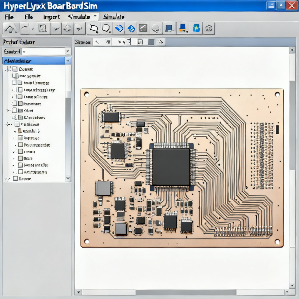
- Action: File > Open > Select your board file.
- Tip: Ensure all stackup information, material properties, and plane layers are correctly defined in the import process.
Step 2: Define the Simulation Configuration
HyperLynx requires clear definitions of signal nets, reference planes, and simulation parameters.
- Select a Net: Choose a high-speed net (e.g., a clock or data line) that you suspect may have return path issues.
- Set the Reference Plane: In the Stackup Editor, verify which plane layer is assigned as the reference for each signal layer. For microstrip lines, the reference is the adjacent plane; for striplines, it is both adjacent planes.
- Configure the Simulation Type: Use Signal Integrity Simulation > Reflection or Crosstalk mode. For return path analysis, Reflection simulation with a fast edge rate (e.g., 200 ps rise time) is most revealing.
Critical Setting: Enable “Include Return Path Effects” in the simulation options. Without this, HyperLynx will assume an ideal, uninterrupted return path, masking real-world issues.
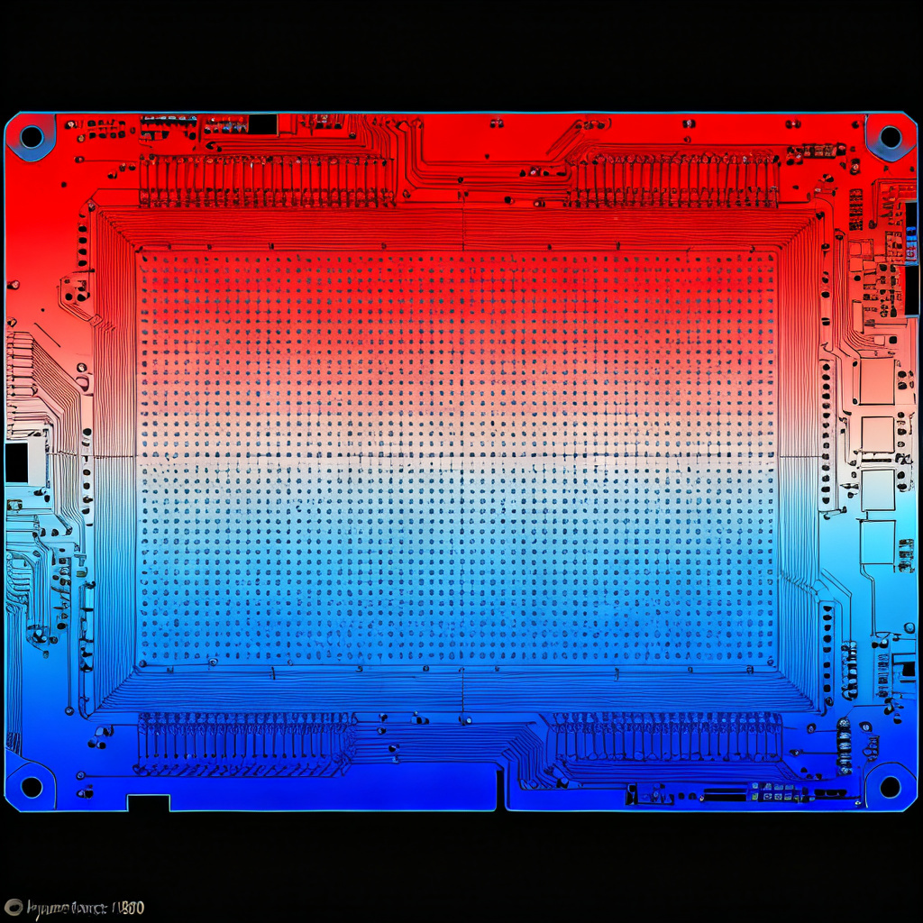
Step 3: Use the Return Path Visualization Tool
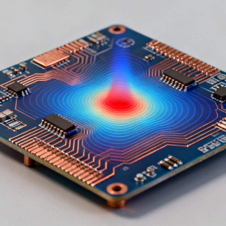
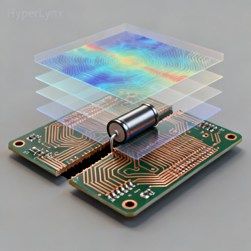
HyperLynx provides a dedicated Return Path Viewer (available in BoardSim and LineSim). This tool graphically plots the return current density on the reference plane for a selected net.
- How to Access: After selecting a net, go to Simulate > Return Path Analysis.
- What You See: A color-coded heat map on the plane layer, where red indicates high return current density and blue indicates low density. Gaps, slots, or plane discontinuities appear as dark voids where current cannot flow.
- Interpretation: A clean return path shows a narrow, continuous red band directly under the signal trace. Any break, widening, or shift in the red band indicates a discontinuity.
Step 4: Run Time-Domain Reflectometry (TDR) Simulation
TDR simulation is a powerful way to correlate return path issues with impedance discontinuities.
- Setup: In the Reflection simulation, set the stimulus to a step pulse (e.g., 0-1V, 200 ps rise time).
- Run TDR: After simulation, view the TDR Impedance Profile. A sudden impedance spike (e.g., from 50Ω to 70Ω) often coincides with a return path gap.
- Cross-Reference: Compare the TDR results with the Return Path Viewer. For example, a 10Ω impedance bump at a via location may correspond to a missing stitching via.
Step 5: Analyze EMI and Crosstalk
Return path discontinuities also degrade EMI and crosstalk performance. HyperLynx allows you to simulate these effects:
- EMI Simulation: Use BoardSim > EMI Analysis to calculate radiated emissions from the net. A large return loop area will show increased emissions at harmonic frequencies.
- Crosstalk Simulation: In Crosstalk mode, place an aggressor net near a victim net. If the return path of the aggressor is broken, the crosstalk coupling to the victim will increase significantly.
3. Practical Simulation Examples and Fixes
Example 1: Crossing a Split Plane
Scenario: A 100 MHz clock trace crosses a gap between two ground islands (e.g., analog and digital GND).
Simulation Steps:
- Select the clock net.
- Open the Return Path Viewer—observe a dark gap where the trace crosses the plane split.
- Run TDR—note an impedance spike from 50Ω to 85Ω at the crossing point.
- Run EMI simulation—see a 15 dB increase in radiated emissions at 200 MHz.
Fix: Add a bridging capacitor (e.g., 0.1 µF) across the split, placed within 100 mils of the crossing. Alternatively, route the trace over a continuous plane, or add a ground bridge (a narrow copper pour connecting the two islands).
Verification in HyperLynx: After adding the capacitor, re-run the Return Path Viewer. The red band should now be continuous across the split, and TDR impedance should return to 50Ω.
Example 2: Via Transition Without Stitching
Scenario: A differential pair transitions from Layer 2 (referenced to GND) to Layer 5 (referenced to VCC). No stitching vias are placed near the signal vias.
Simulation Steps:
- Select one of the differential traces.
- In the Return Path Viewer, note that the return current path on Layer 2 (GND) ends abruptly at the via. On Layer 5 (VCC), the return current must find a new path, often through a distant decoupling capacitor.
- TDR shows a negative impedance dip (e.g., from 50Ω to 35Ω) at the via, indicating increased capacitance due to the return current loop.
- Crosstalk simulation reveals increased coupling to adjacent traces.
Fix: Add stitching vias connecting GND and VCC planes within 50 mils of the signal vias. Use multiple vias (e.g., 2-3) to reduce inductance. Ensure the stitching vias are placed symmetrically for differential pairs.
Verification: After adding stitching vias, the Return Path Viewer should show a continuous current transition from GND to VCC. TDR impedance should return to 50Ω, and crosstalk should drop by 5-10 dB.
Example 3: Reference Plane Switch Without AC Coupling
Scenario: A signal net switches from a ground reference to a power reference (e.g., 3.3V plane) without a nearby AC coupling capacitor.
Simulation Steps:
- Select the net and run Reflection simulation. Observe a large impedance discontinuity (e.g., from 50Ω to 100Ω) at the transition point.
- The Return Path Viewer shows that the return current on the power plane is weak and diffuse, indicating high impedance.
- EMI simulation shows a sharp emission peak at the signal’s fundamental frequency.
Fix: Place a decoupling capacitor (e.g., 0.1 µF) between the power and ground planes near the transition point. This provides a low-impedance path for the return current to flow from the power plane back to the ground plane.
Verification: Re-run simulations. TDR impedance should stabilize, and return current density on the power plane should increase and concentrate under the trace.
4. Advanced Techniques and Best Practices
Using Differential Pair Analysis
For differential signals, the return path is less critical because the return current flows primarily in the complementary trace. However, common-mode return current can still cause issues. HyperLynx’s Differential Pair Wizard allows you to simulate both differential and common-mode return paths.
- Best Practice: For differential pairs, ensure that the reference plane is continuous and that stitching vias are placed symmetrically for both traces.
Optimizing Stitching Via Placement
HyperLynx includes a Via Stitching Optimization feature (in BoardSim). It automatically suggests stitching via locations based on return current density maps.
- How to Use: After running Return Path Analysis, select Tools > Via Stitching Optimization. HyperLynx will propose via locations and simulate the improvement in impedance and EMI.
- Rule of Thumb: Place stitching vias at a spacing of less than λ/20 (where λ is the wavelength of the highest harmonic frequency). For a 1 GHz signal, this is approximately 150 mils (3.8 mm).
Simulating Plane Resonance
Return path discontinuities can also excite plane resonances. HyperLynx’s Plane Resonance Analyzer (available in BoardSim) calculates the resonant frequencies of power and ground planes.
- Application: If a return path gap creates a large loop, that loop may resonate at a harmonic of the signal frequency, amplifying EMI.
- Fix: Add decoupling capacitors or increase plane capacitance to dampen resonances.
Validating with Measurements
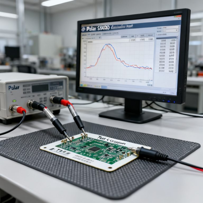
While simulation is powerful, final validation with physical measurements (e.g., using a vector network analyzer or TDR oscilloscope) is recommended. HyperLynx can export simulation results (e.g., S-parameters) for comparison with measurements.
5. Common Pitfalls and How to Avoid Them
Pitfall 1: Ignoring the Return Path for Power Nets
Many designers focus only on signal return paths, but power distribution network (PDN) return paths are equally important. High-speed switching currents from ICs need a low-inductance return path through the power plane.
HyperLynx Solution: Use Power Integrity Simulation (available in HyperLynx PI) to analyze PDN return paths. Ensure that power and ground planes are tightly coupled (thin dielectric) and that vias are placed near IC power pins.
Pitfall 2: Overlooking Return Path in Multi-Layer Boards
In boards with more than four layers, the return path may involve multiple reference planes. For example, a signal on Layer 1 may reference Layer 2 (GND) but also couple to Layer 3 (VCC) if the dielectric between Layer 2 and Layer 3 is thin.
HyperLynx Solution: Use the Stackup Editor to define all coupling coefficients. Enable Multi-Reference Plane Analysis in the Return Path Viewer to see how return current distributes across multiple planes.
Pitfall 3: Relying Only on TDR Without Visual Inspection
TDR can indicate an impedance discontinuity, but it does not show the root cause. Always combine TDR with the Return Path Viewer to identify the exact location and nature of the problem.
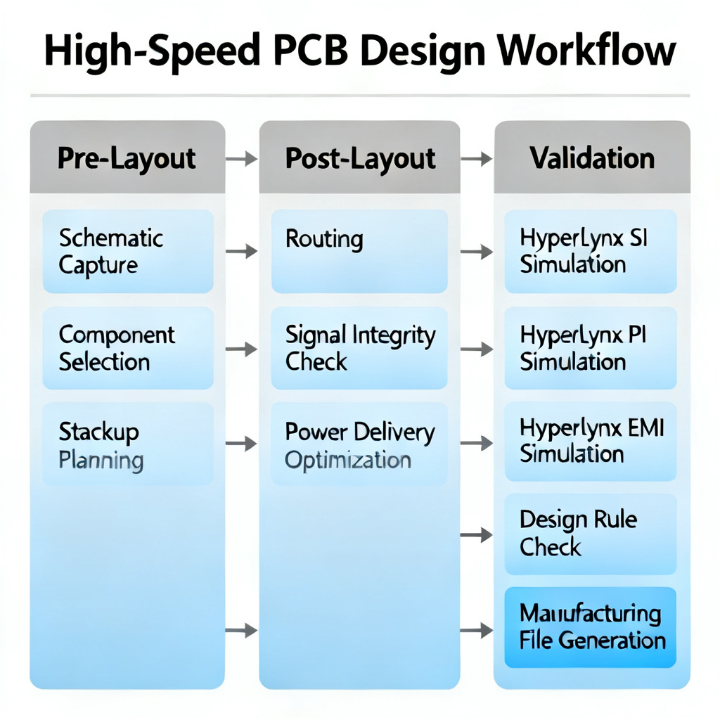
6. Conclusion: Integrating Return Path Analysis into Your Design Flow
Return path design simulation in HyperLynx is not a one-time task; it should be integrated into every stage of high-speed PCB design:
- Pre-Layout (LineSim): Use HyperLynx LineSim to evaluate different stackups, plane configurations, and via strategies before committing to layout.
- Post-Layout (BoardSim): After routing, run Return Path Viewer and TDR on critical nets. Fix any discontinuities before finalizing the design.
- Final Validation: Run EMI and crosstalk simulations to ensure the design meets regulatory and performance requirements.
By mastering these techniques, you will significantly reduce SI and EMI issues, leading to faster design cycles, lower costs, and higher reliability. HyperLynx provides the tools; this guide provides the roadmap. Apply these principles to your next high-speed PCB design, and you will see the difference in first-pass success.
Frequently Asked Questions (FAQ)
What is a return path in high-speed PCB design?
A return path is the route taken by the return current of a signal. In high-speed PCB design, it is essential for maintaining signal integrity and minimizing EMI.
How does HyperLynx help with return path simulation?
HyperLynx provides the Return Path Viewer and TDR simulation to visualize and analyze return current flow, helping engineers identify and fix discontinuities in the return path.
What are common return path discontinuities?
Common issues include split planes, via transitions without stitching, reference plane changes, and cutouts or moats in the plane layers.
Why is return path important for high-speed PCB design?
A clean return path ensures low inductance, consistent impedance, and reduced crosstalk and EMI, which are critical for high-speed signal integrity.
How can I fix a return path discontinuity in HyperLynx?
Fixes include adding stitching vias, bridging capacitors, ground bridges, or adjusting the stackup to create a continuous reference plane.
| Parameter | Description | Recommended Value for Return Path Analysis |
|---|---|---|
| Rise Time | Edge rate of the simulated signal | 200 ps (for high-speed signals) |
| Reference Plane | Plane layer assigned as return path | Adjacent solid plane (GND or VCC) |
| Stitching Via Spacing | Distance between stitching vias | < λ/20 (e.g., 150 mils at 1 GHz) |
| Bridging Capacitor Value | Capacitance for split plane bridge | 0.1 µF (low ESL) |
Industry Terminology
- Return Path: The conductive route that carries the return current of a signal, typically through a reference plane.
- Stitching Via: A via connecting two reference planes to provide a low-inductance return path for signals transitioning layers.
- TDR (Time Domain Reflectometry): A measurement technique used to characterize impedance variations in a transmission line.
- EMI (Electromagnetic Interference): Unwanted radiated energy from a circuit, often exacerbated by poor return paths.
- Reference Plane: A continuous conductive layer (ground or power) that serves as the return path for signal traces.