Mastering return path PCB design analysis in Cadence Sigrity is essential for high-speed signal integrity. This step-by-step guide integrates expert techniques from top-ranked sources to help B2B PCB manufacturers and engineers optimize return paths, reduce EMI, and ensure reliable custom PCB production.
Step 1: Prepare Your PCB Design for Return Path Analysis
Before starting return path PCB design analysis in Cadence Sigrity, ensure your PCB layout is optimized for simulation. This step involves importing your design and setting up the environment.
1.1 Import the PCB Layout
Use Cadence OrCAD PCB Editor or Allegro to export your design in .brd or .mcm format. For Sigrity, convert to .spd (Sigrity PCB Database) via the Sigrity Workflow Manager. Pro Tip: Ensure all layers are correctly defined, especially ground and power planes, as these are critical for return path analysis.
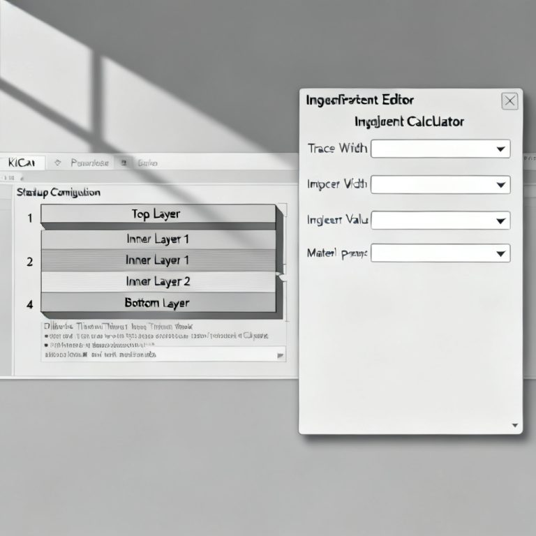
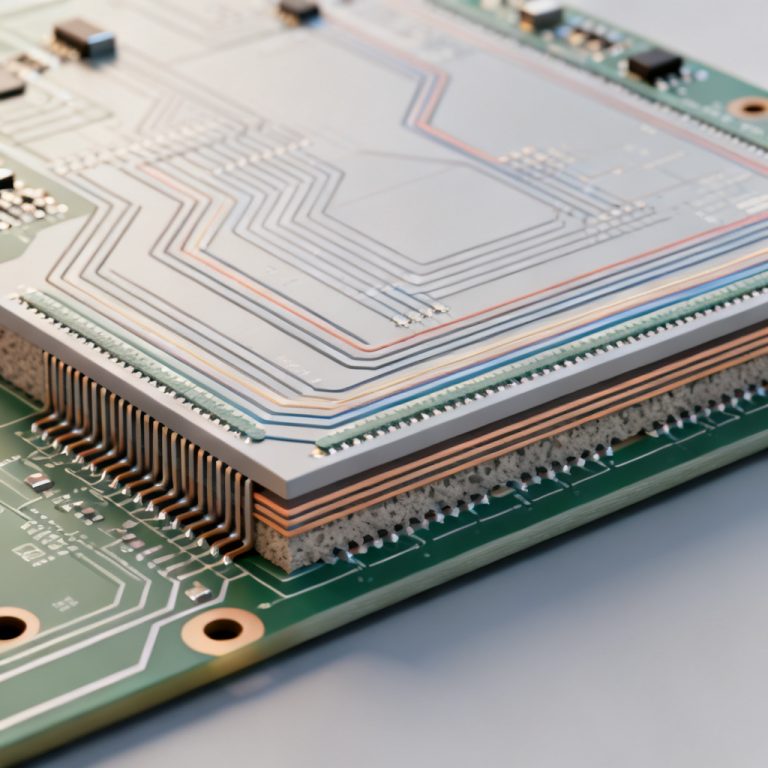
1.2 Define Stackup and Materials
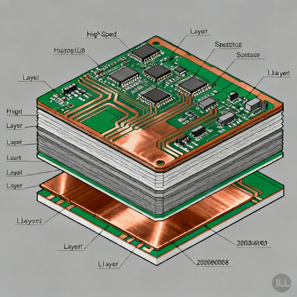
In Sigrity, navigate to Stackup Editor (under Setup > Stackup). Assign material properties (e.g., FR4 with dielectric constant 4.2, loss tangent 0.02 for high-speed designs). Set copper thickness (e.g., 1 oz or 2 oz for high-current paths) and prepreg thickness between layers. For high-speed signals (e.g., 10 Gbps), minimize dielectric thickness to reduce impedance.
1.3 Identify Critical Nets
Use Net Manager to highlight high-speed nets (e.g., DDR, PCIe, or Ethernet traces). Label them as “Critical” for focused analysis. This step, from expert sources, emphasizes that not all nets require deep return path analysis; prioritize those with fast rise times (<1 ns).
Step 2: Run Initial Return Path Simulation with Sigrity PowerSI
Sigrity PowerSI is the primary tool for frequency-domain analysis of return paths in return path PCB design analysis in Cadence Sigrity. Here’s how to execute it.
2.1 Launch PowerSI
From Sigrity Workflow Manager, select PowerSI and choose Frequency Domain Simulation. Set frequency range: For high-speed designs, use 1 MHz to 20 GHz (or up to the 5th harmonic of your signal frequency). For example, for a 5 GHz signal, analyze up to 25 GHz.
2.2 Configure Simulation Settings
Excitation Setup: Apply a 1V AC source to the signal net and its return path (e.g., ground plane). Use Port Setup to define single-ended or differential ports. Return Path Reference: In Reference Plane Settings, select the nearest ground or power plane. For high-speed designs, use a solid plane (no splits) to avoid impedance discontinuity.
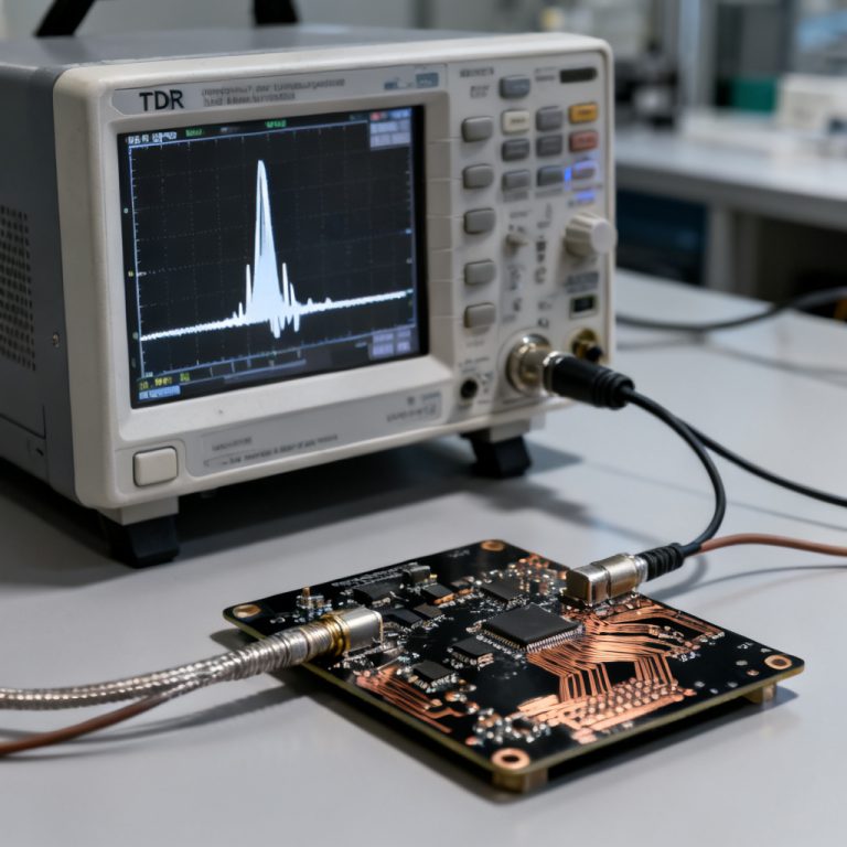
2.3 Run the Simulation
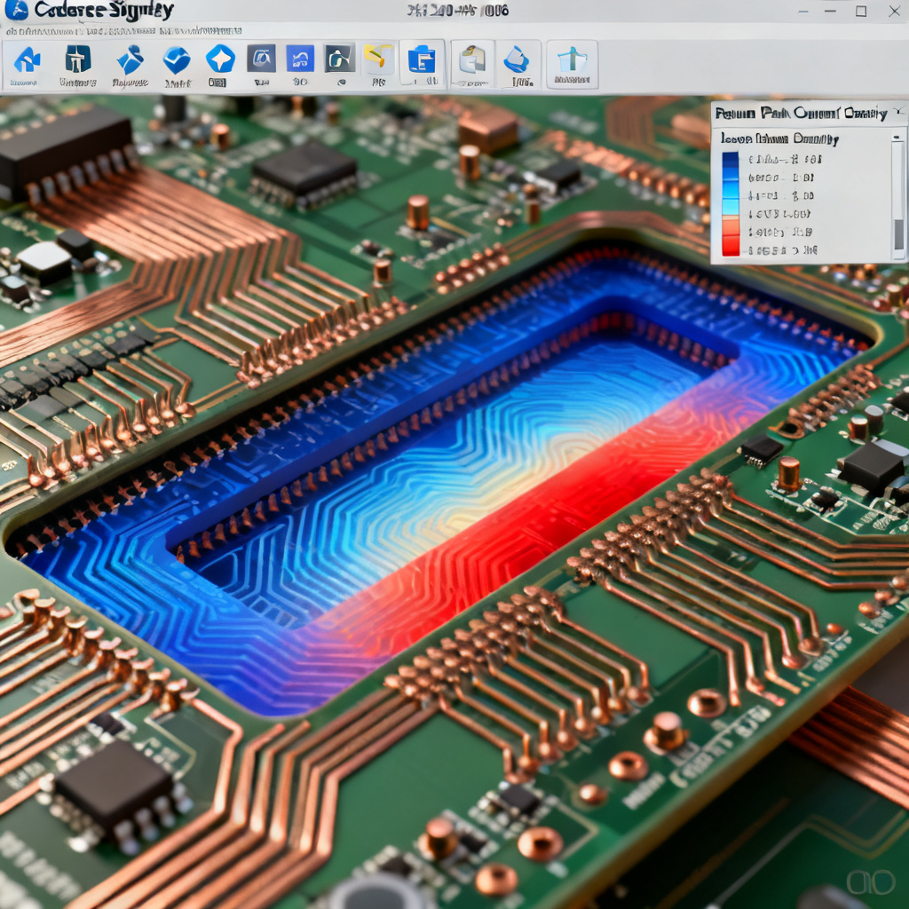
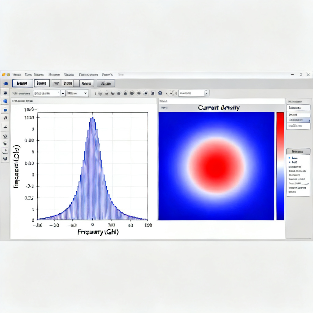
Click Simulate and monitor progress. PowerSI will compute S-parameters, impedance profiles, and current density maps. Key Output: The Return Path Current Density plot shows where current flows. Discontinuities (e.g., near vias or slots) appear as hot spots.
2.4 Analyze Results
Impedance Profile: Check for impedance spikes > 10% above target (e.g., target 50Ω for single-ended traces). High impedance indicates poor return path. Current Density: Use Visualizer to overlay current vectors. If current deviates from the expected path (e.g., around a split plane), redesign the layout.
Step 3: Perform 3D Return Path Analysis with Sigrity SpeedXP
For complex geometries (e.g., via transitions, BGA breakout regions), Sigrity SpeedXP provides 3D EM simulation for accurate return path modeling in return path PCB design analysis in Cadence Sigrity.
3.1 Export to SpeedXP
From PowerSI results, select Export to SpeedXP for 3D analysis. Alternatively, import the .spd file directly. Expert Insight: Use SpeedXP for via arrays or connector transitions where 2D analysis fails.
3.2 Set Up 3D Simulation
Mesh Settings: Use Adaptive Meshing with a maximum mesh size of 1/10th of the shortest wavelength (e.g., for 10 GHz, mesh < 3 mm). Boundary Conditions: Apply Perfectly Matched Layers (PML) to absorb reflections at simulation boundaries.
3.3 Run and Interpret Results
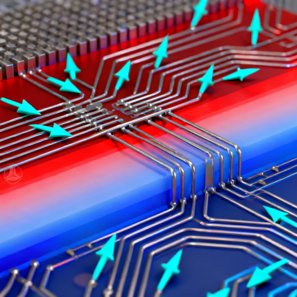
Execute Time-Domain Reflectometry (TDR) simulation to visualize impedance changes along the return path. A TDR plot showing impedance dips (e.g., from 50Ω to 30Ω) indicates return path discontinuities. Current Flow Visualization: Use 3D Field Viewer to see current loops. For example, a via transition should show current flowing through adjacent ground vias; if not, add stitching vias.
3.4 Mitigation Strategies
Add Stitching Vias: Place ground vias within 1/20th of the signal wavelength from the signal via to ensure a low-impedance return path. Avoid Split Planes: Re-route critical nets over continuous ground planes. If splits are unavoidable, use bridge capacitors (e.g., 0.1 μF) to connect split planes.
Step 4: Validate Return Path with Sigrity SystemSI
For system-level analysis (e.g., multi-board designs), Sigrity SystemSI validates return path across connectors and cables in return path PCB design analysis in Cadence Sigrity.

4.1 Import System Components
Use SystemSI Model Manager to include IBIS models for drivers and receivers. Assign Power Delivery Network (PDN) models for each board. Note: For B2B custom PCB orders, ensure models match your customer’s specifications (e.g., 1.8V for DDR4).
4.2 Run Transient Simulation
Set up Transient Analysis with a pseudo-random bit sequence (PRBS) pattern (e.g., PRBS7 for 10 Gbps). Monitor eye diagrams and return path current. Key Metric: Eye height > 200 mV and jitter < 0.1 UI indicate good return path integrity.
4.3 Optimize Based on Results
If eye diagram shows closure, check return path via Signal Integrity Report. Common fixes: increase ground via count or widen trace width to reduce inductance.
Step 5: Document and Iterate for Manufacturing
The final step bridges analysis to production, critical for B2B PCB sales in return path PCB design analysis in Cadence Sigrity.
5.1 Generate Reports
Use Sigrity Report Generator to create PDFs with impedance profiles, current density maps, and TDR plots. Include recommendations (e.g., “Add 3 stitching vias near U1 pin A1”). B2B Tip: Attach these reports to your quotation to demonstrate technical expertise.
5.2 Design Rule Checks (DRC)
Export results back to Allegro for DRC. Common rules: minimum ground via spacing (e.g., 20 mils for 10 Gbps) and no slots under critical nets.
5.3 Iterate for Custom Orders
For customer-specific high-speed PCBs (e.g., 12-layer with 0.5 mm pitch BGA), run a second iteration with adjusted stackup (e.g., lower DK material like Rogers 4350B). Use Sigrity’s Optimization Tool to automate via placement.
Common Pitfalls and Expert Solutions in Return Path Analysis
| Parameter | Issue | Solution |
|---|---|---|
| Power plane return path | High-frequency noise | Use AC-coupled ground plane |
| Via stub length | Resonance at 10+ GHz | Backdrill stubs > 10 mils |
| Simulation frequency step | Missed anomalies | Set step < 100 MHz |
Comparing Return Path Analysis Tools: Sigrity vs. Alternatives
While tools like Ansys Q2D Extractor and Polar Si9000 offer impedance calculations, Cadence Sigrity excels in comprehensive return path PCB design analysis by integrating frequency-domain, 3D EM, and system-level simulations in one workflow. This reduces iteration time for custom high-speed PCB orders.
Key Terminology for Return Path PCB Design
Return path discontinuity: A break in the low-impedance path causing signal reflection. Stitching via: A ground via placed near signal vias to maintain return path continuity. Impedance control: Managing trace impedance to match target values (e.g., 50Ω).
FAQ: Return Path PCB Design Analysis in Cadence Sigrity
What is return path in PCB design?
The return path is the route current takes to return to its source, typically through a ground or power plane. In high-speed designs, a continuous return path minimizes EMI and signal integrity issues.
How does Cadence Sigrity analyze return paths?
Cadence Sigrity uses tools like PowerSI for frequency-domain analysis and SpeedXP for 3D EM simulation to visualize current density and impedance profiles, enabling engineers to identify and fix return path discontinuities.
Why is return path analysis important for high-speed PCBs?
Poor return paths cause signal reflections, increased crosstalk, and electromagnetic interference. For B2B custom PCB manufacturing, ensuring a robust return path is critical for signal integrity at data rates above 1 Gbps.
What are common return path issues in multilayer PCBs?
Common issues include split planes, insufficient stitching vias, and via stubs. These can be detected using TDR simulations in Sigrity SpeedXP and mitigated with proper layout techniques.
How can I optimize return path for custom PCB orders?
Use Sigrity’s optimization tools to automate via placement and adjust stackup materials. Document simulation results in reports to build client trust and demonstrate technical capability.
Conclusion: Elevate Your High-Speed PCB Design with Sigrity
Mastering return path PCB design analysis in Cadence Sigrity is a competitive advantage for B2B PCB manufacturers. By following this step-by-step guide—preparing your design, running PowerSI for initial scans, using SpeedXP for 3D validation, and SystemSI for system-level checks—you ensure signal integrity, reduce EMI, and deliver reliable high-speed PCBs. For custom orders, iterate based on simulation results and document every step to build client trust.
Call to Action: Ready to optimize your high-speed PCB design? Contact our engineering team for a free Sigrity analysis consultation and get a quote for your custom PCB order today.