Simulating PDN impedance using Power Integrity PCB tools is essential for high-speed PCB design, ensuring stable power delivery and signal integrity. This guide provides a comprehensive, step-by-step approach to mastering PDN impedance simulation, from fundamentals to advanced optimization techniques, tailored for B2B engineers seeking reliable custom high-speed PCB manufacturing.
1. Understanding PDN Impedance and Its Role in Power Integrity
1.1 What is PDN Impedance?
PDN impedance is the frequency-dependent resistance and reactance seen by a device (e.g., an FPGA or ASIC) looking into its power supply network. It is measured between the power and ground planes at the device’s power pins. The goal is to keep this impedance below a target value across all operating frequencies to maintain a stable voltage within the specified tolerance (typically ±5% or ±3% for high-speed designs).
1.2 The Frequency Spectrum of PDN Behavior
- Low Frequencies (DC to ~100 kHz): Dominated by the voltage regulator module (VRM) output impedance and bulk decoupling capacitors.
- Mid Frequencies (100 kHz to ~10 MHz): Governed by ceramic capacitors (MLCCs) and their equivalent series resistance (ESR) and inductance (ESL).
- High Frequencies (>10 MHz to >1 GHz): Controlled by the plane capacitance between power and ground layers, as well as package and on-die capacitance.
1.3 The Critical Concept: Target Impedance
The target impedance (Z_target) is the maximum allowable impedance that the PDN can present to the load. It is calculated using: Z_target = (V_dd × Ripple Tolerance) / ΔI_transient. For example, a 1.8V rail with 5% ripple tolerance and a 2A transient current yields a target impedance of 45 mΩ. Exceeding this value causes voltage droops that can corrupt logic states in high-speed circuits.
2. Overview of Power Integrity PCB Tools for PDN Simulation
2.1 Types of PI Tools
Three primary tool categories are used in industry:
- 2D Field Solvers (e.g., Ansys SIwave, Cadence Sigrity PowerSI): Ideal for analyzing plane impedance, resonance, and decoupling capacitor placement. They model the PCB as a planar structure.
- 3D Full-Wave Solvers (e.g., CST Studio Suite, HFSS): Necessary for high-frequency effects, via modeling, and complex geometries like BGA breakout regions.
- Hybrid/Integrated Tools (e.g., Keysight ADS, Altium PDN Analyzer): Combine circuit simulation with EM analysis for system-level PDN design.
2.2 Selecting the Right Tool for Your High-Speed PCB
- For initial design and optimization: Use a 2D field solver with fast simulation times (e.g., Cadence Sigrity PowerSI).
- For final verification of critical nets: Use a 3D solver to capture via inductance and plane coupling.
- For B2B custom PCB manufacturing: Always validate with a tool that supports industry-standard models (e.g., SPICE models for VRM and capacitors).
3. Step-by-Step Guide to Simulating PDN Impedance
Step 1: Prepare the PCB Stack-Up and Geometry
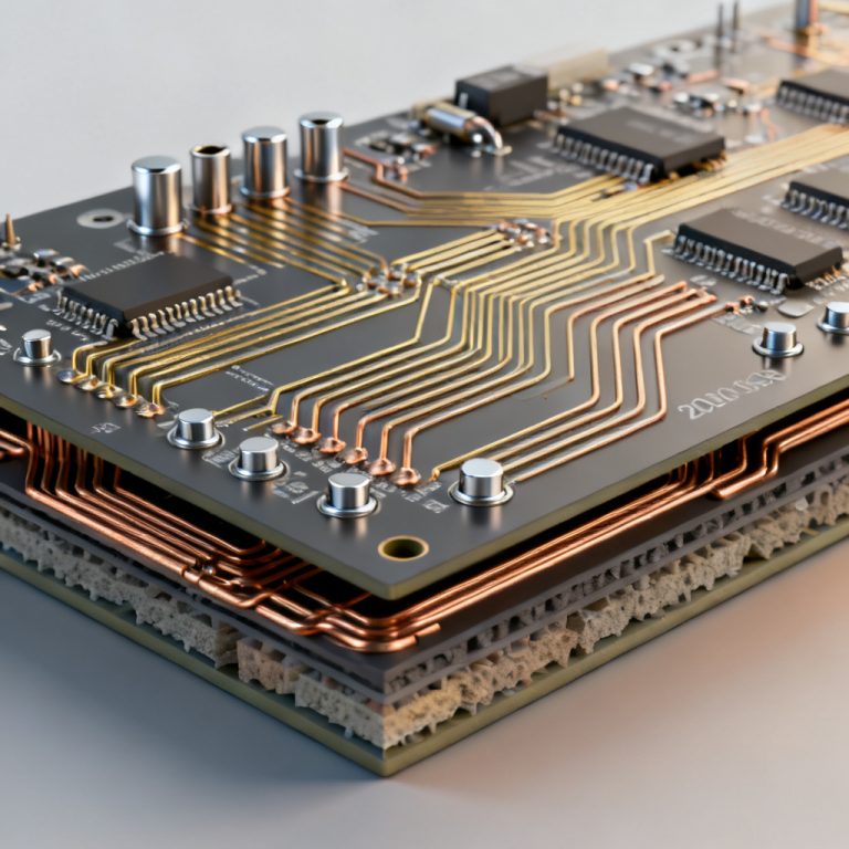
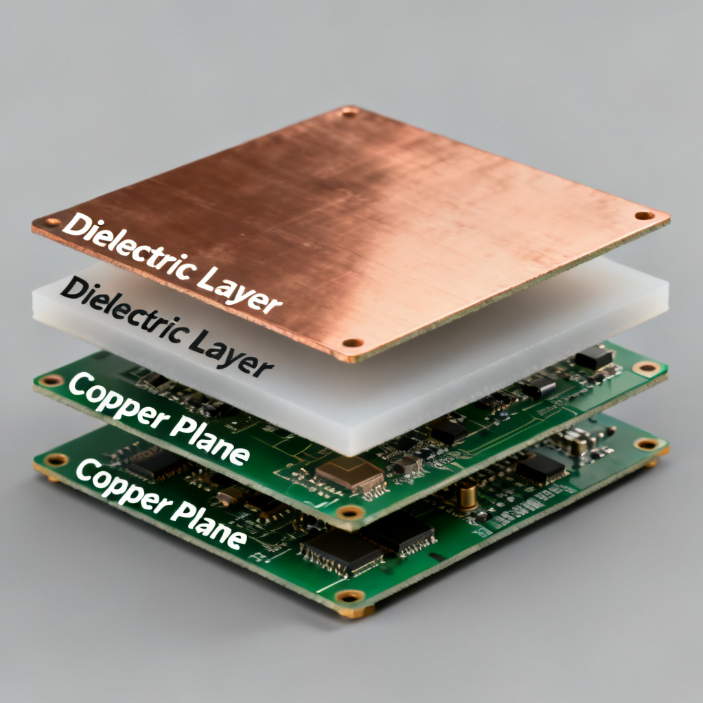
Define the stack-up for Power Integrity PCB, including layer thickness, dielectric material (e.g., FR4, Rogers), and copper weight. For high-speed designs, use thin dielectrics (e.g., 100 µm) between power and ground planes to maximize plane capacitance. Import the layout using Gerber or ODB++ files, ensuring all power and ground shapes are correctly identified. Set material properties, input dielectric constant (Dk) and loss tangent (Df) for each layer. For high-speed PCBs, low-loss materials (e.g., Rogers 4350B) are preferred.
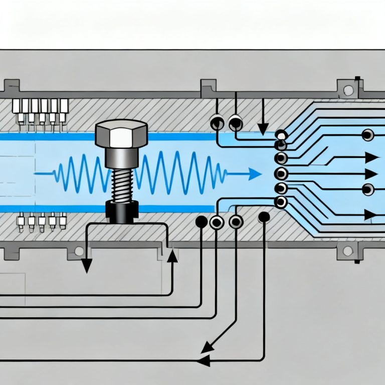
Step 2: Define Ports and Excitation
Place ports at the load (IC) location using a single-ended port between power and ground pins. For multi-pin devices (e.g., BGA), create multiple ports or a single port at the centroid. Set the frequency sweep from 1 kHz to 10 GHz or higher, using a logarithmic sweep for broad analysis and a linear sweep for resonance peaks.
Step 3: Model the VRM and Decoupling Capacitors
Use a simple R-L circuit (e.g., 1 mΩ resistance, 10 nH inductance) or a manufacturer-provided SPICE model for the VRM. The VRM dominates low-frequency impedance. For capacitors, include ESL, ESR, and capacitance values for each decoupling cap. Use accurate models from reputable vendors (e.g., Murata, TDK) and place capacitors in the simulation at their exact physical locations.
Step 4: Run the Simulation
Execute the simulation, which may be a frequency-domain sweep (S-parameter extraction) or a transient analysis. For 3D solvers, ensure mesh refinement is sufficient at high frequencies (e.g., at least 10 cells per wavelength).
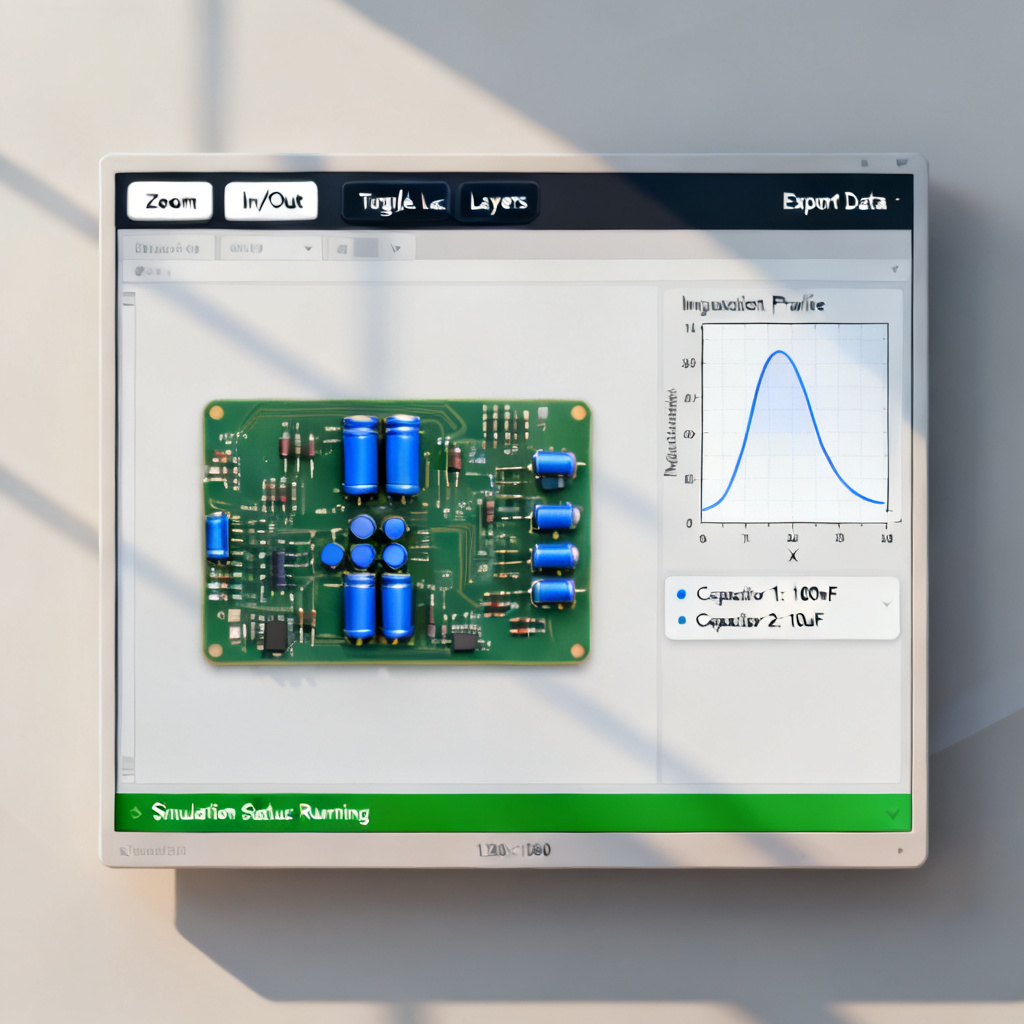
Step 5: Analyze the Impedance Profile
Plot Z11 (impedance at port 1) vs. frequency. The ideal curve should be flat and below Z_target across the entire frequency range. Identify resonance peaks, which indicate high-impedance points caused by plane resonance or capacitor anti-resonance. Check for inductive behavior; above ~100 MHz, the impedance should rise linearly due to plane and via inductance. If the slope is too steep, the PDN is inductive.
Step 6: Optimize Based on Results
Add or relocate decoupling capacitors to target resonance frequencies by placing capacitors with lower ESL closer to the IC. Adjust plane capacitance using thinner dielectrics or add embedded capacitance materials (e.g., FaradFlex) to lower high-frequency impedance. Reduce via inductance by using multiple vias in parallel for power/ground connections and minimizing via length.
4. Interpreting Simulation Results and Common Pitfalls
4.1 Key Metrics to Verify
- DC Resistance (DCR): Should be < 10 mΩ for high-current rails. High DCR causes I²R losses.
- First Resonant Frequency: Typically occurs between 10–100 MHz. A low first resonance indicates excessive inductance.
- Impedance at IC Switching Frequency: Ensure Z is below Z_target at the fundamental and first few harmonics of the clock frequency.
4.2 Common Mistakes and How to Avoid Them
| Mistake | Consequence | Solution |
|---|---|---|
| Ignoring via inductance | Underestimates high-frequency impedance | Model vias explicitly or use 3D solvers |
| Using ideal capacitor models | Misses anti-resonance peaks | Use vendor SPICE models with ESL/ESR |
| Neglecting VRM output impedance | Inaccurate low-frequency behavior | Include VRM model with output capacitance |
| Overlooking plane resonance | Unexpected impedance spikes | Check modal analysis or use damping capacitors |
4.3 Real-World Example: High-Speed FPGA PDN
A typical high-speed FPGA requires Z_target < 50 mΩ up to 500 MHz. Simulation reveals a 120 mΩ peak at 200 MHz due to anti-resonance between 10 µF and 0.1 µF capacitors. Solution: Replace the 0.1 µF cap with a 0.01 µF cap having lower ESL, and add a 1 µF cap in a different location to shift the anti-resonance.
5. Advanced Techniques for High-Speed PCB PDN Optimization
5.1 Using Embedded Capacitance
Embedded capacitance materials (e.g., 3M C-Ply, FaradFlex) create a distributed plane capacitance of 1–10 nF/in². This eliminates the need for many discrete capacitors and provides ultra-low impedance above 100 MHz. Simulation must include the material’s Dk and thickness.
5.2 Multi-Node PDN Analysis
For complex designs with multiple ICs, simulate the PDN impedance at each critical load. Use a network of ports and analyze the transfer impedance (Z12, Z13) between loads to identify coupling issues.
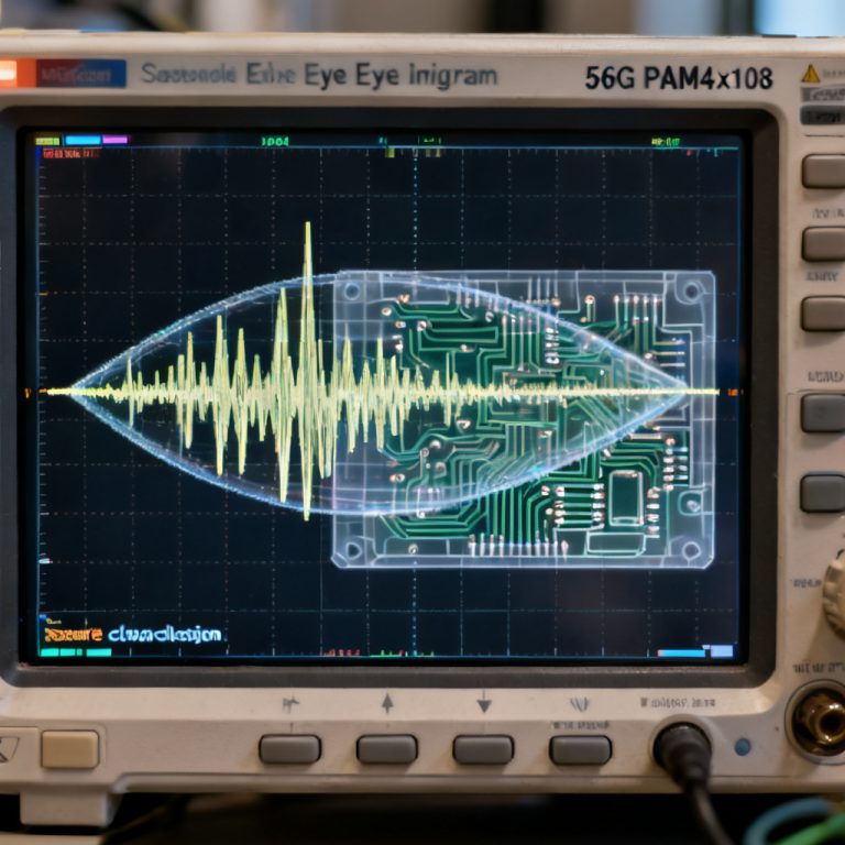
5.3 Time-Domain Transient Simulation
Frequency-domain impedance analysis is necessary but not sufficient. Run a transient simulation with a realistic current profile (e.g., step load, periodic burst) to observe voltage ripple. A transient simulation reveals whether the PDN can respond quickly enough to rapid current changes.
5.4 Correlation with Measurement
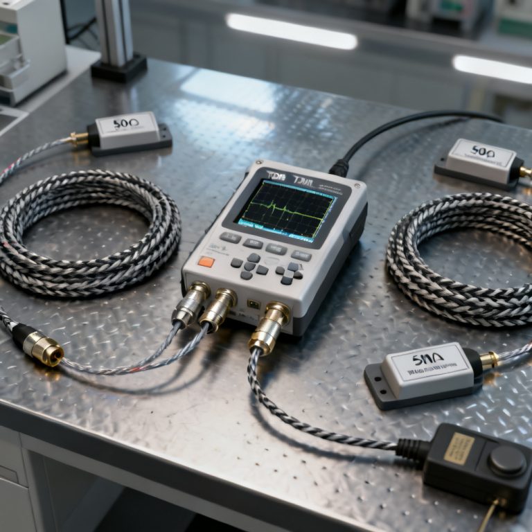
Always validate simulation results with physical measurements using a Vector Network Analyzer (VNA) or impedance analyzer. Common discrepancies arise from unmodeled parasitics (via stubs, solder bumps, and package inductance), capacitor tolerance (actual capacitance can vary ±20% from nominal), and temperature effects (ESR increases with temperature).
6. Best Practices for B2B High-Speed PCB Manufacturing
For B2B clients ordering custom high-speed PCBs, the following guidelines ensure PDN simulation translates to reliable hardware:
- Provide the PDN simulation report to your PCB manufacturer, including target impedance, simulated profile, and decoupling capacitor BOM.
- Specify stack-up requirements for plane capacitance (e.g., “core thickness between PWR and GND layers: 100 µm ±10%”).
- Request controlled impedance for all high-speed traces, and ensure PDN planes have no slots or splits.
- Use low-ESR capacitors from trusted brands (e.g., Murata GRM series) and avoid high-ESR tantalum capacitors for decoupling.
- Design for manufacturability (DFM): Avoid placing capacitors too close to vias or under large components where soldering is difficult.
FAQ: Simulating PDN Impedance Using Power Integrity PCB Tools
What is the first step to simulate PDN impedance using Power Integrity PCB tools?
The first step is to prepare the PCB stack-up and geometry, defining layer thickness, dielectric materials, and importing the layout to ensure accurate modeling of the power distribution network.
Why is target impedance critical in PDN impedance simulation?
Target impedance is critical because it defines the maximum allowable impedance to maintain stable voltage; exceeding it causes voltage droops that degrade signal integrity in high-speed PCBs.
How do I optimize PDN impedance after simulation?
Optimize by adding or relocating decoupling capacitors, adjusting plane capacitance with thinner dielectrics, and reducing via inductance through parallel vias, all while using Power Integrity PCB tools to verify improvements.
What are common mistakes in PDN impedance simulation?
Common mistakes include ignoring via inductance, using ideal capacitor models, neglecting VRM output impedance, and overlooking plane resonance, which can be avoided with accurate modeling and 3D solvers.
How does PDN impedance simulation benefit B2B high-speed PCB manufacturing?
It ensures reliable power delivery, reduces design iterations, and provides a documented simulation report that helps PCB manufacturers meet stringent impedance and performance requirements for custom high-speed PCBs.
Conclusion: The Path to a Robust PDN
Simulating PDN impedance using Power Integrity tools is a non-negotiable step in high-speed PCB design. By following the step-by-step methodology outlined in this guide—from stack-up preparation to advanced optimization—you can ensure your custom PCB meets the stringent power delivery requirements of modern FPGAs, ASICs, and RF modules. Key takeaways include always defining a target impedance based on your IC’s specifications, using accurate models for VRM, capacitors, and vias, validating simulation results with transient analysis and physical measurements, and partnering with a PCB manufacturer experienced in high-speed design to ensure your PDN simulation translates to real-world performance. For B2B clients requiring high-speed PCBs with optimized PDN performance, our team offers free design review and PDN simulation support. Contact us to discuss your next project.