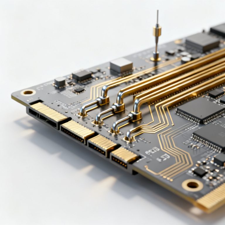
In high-speed PCB design for DDR memory interfaces, Crosstalk in High Speed PCB for DDR Interfaces is the primary cause of timing violations and data corruption. While both the Address Bus and Data Bus are susceptible, the nature of interference differs fundamentally. This guide provides comprehensive mitigation strategies for B2B PCB manufacturers and designers.
Fundamentals of Crosstalk in High Speed PCB for DDR Interfaces
What is Crosstalk and Why Does it Matter for DDR?
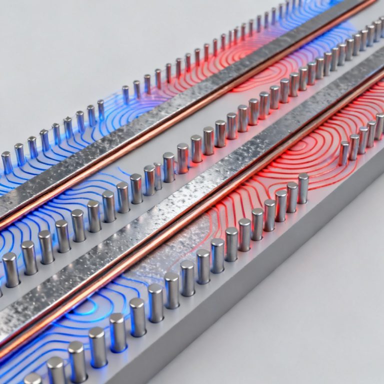
Crosstalk in High Speed PCB for DDR Interfaces refers to unwanted electromagnetic coupling between adjacent traces. At DDR frequencies exceeding 800 MHz, this coupling causes timing jitter, voltage margin reduction, and data-dependent errors. The severity depends on coupling length, edge rates (often under 100 ps), and trace proximity.
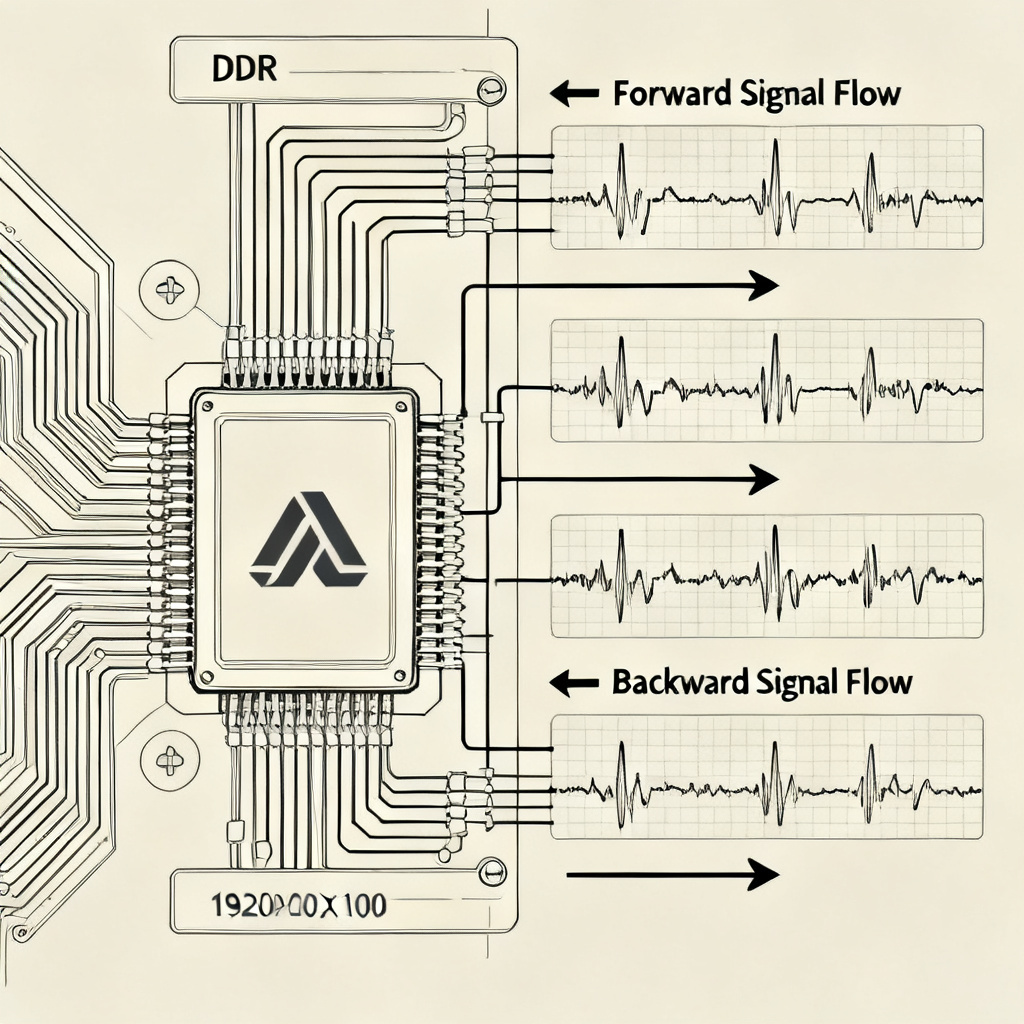
Forward vs. Backward Crosstalk
Understanding crosstalk types is essential for modeling DDR interfaces. Backward (Near-End) Crosstalk dominates PCB traces, causing pulse widths equal to twice the propagation delay. Forward (Far-End) Crosstalk is most problematic in microstrip layers due to inhomogeneous dielectrics.
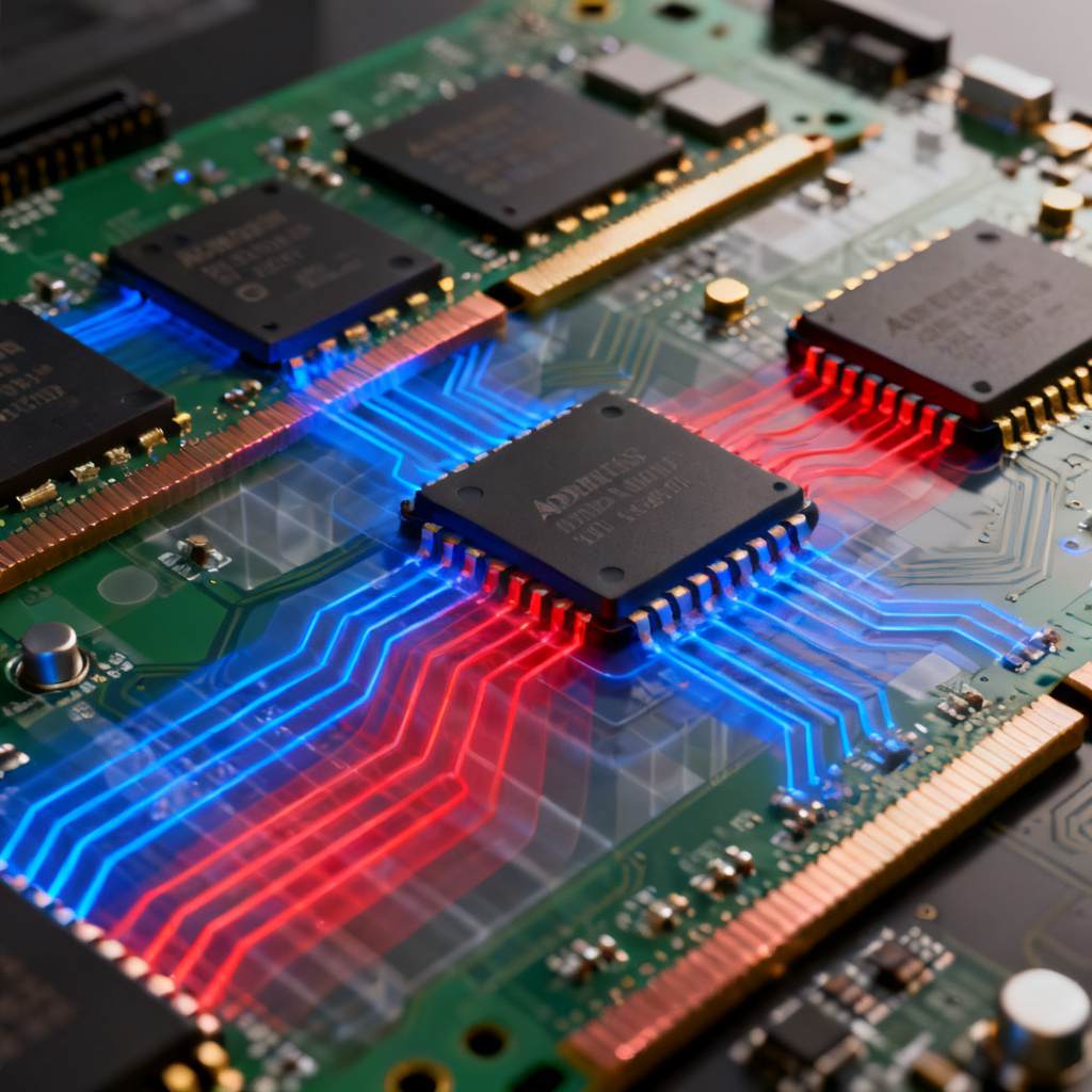
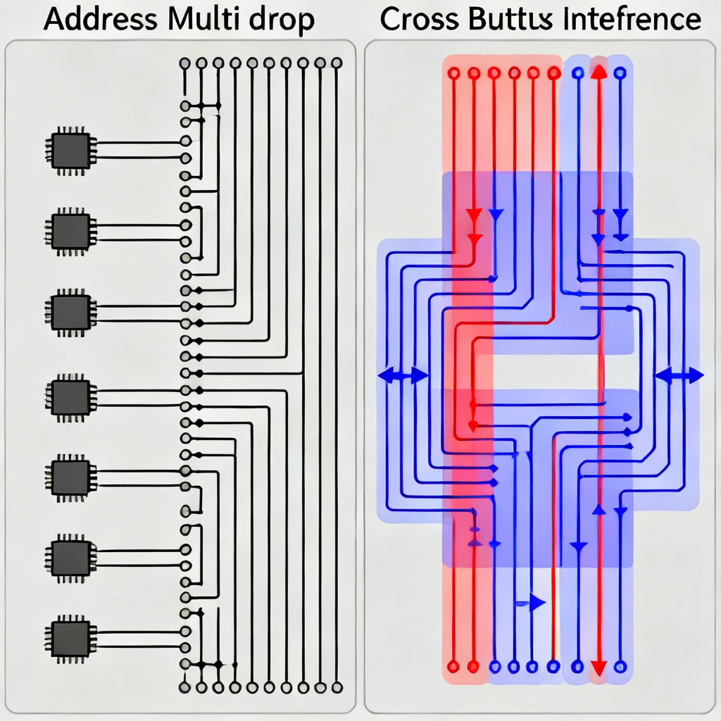
Address Bus vs. Data Bus: Crosstalk Analysis for High Speed PCB
The Address Bus: Multi-Drop Topology Challenges
The address bus uses a one-to-many topology, where a single signal reaches multiple DRAM chips. Crosstalk in High Speed PCB for DDR Interfaces on the address bus is exacerbated by long parallel traces, stub effects from vias, and simultaneous switching noise. Mitigation requires fly-by topology, 4W to 5W spacing, and stripline routing.
The Data Bus: Bidirectional Interference
The bidirectional data bus creates unique crosstalk scenarios. Simultaneous Switching Output effects cause ground bounce that couples onto all DQ lines. Byte lane isolation, trace length matching within 10-20 mils, and On-Die Termination are critical for controlling Crosstalk in High Speed PCB for DDR Interfaces on the data bus.
Modeling and Simulation for Crosstalk in High Speed PCB
Field Solvers: The Gold Standard
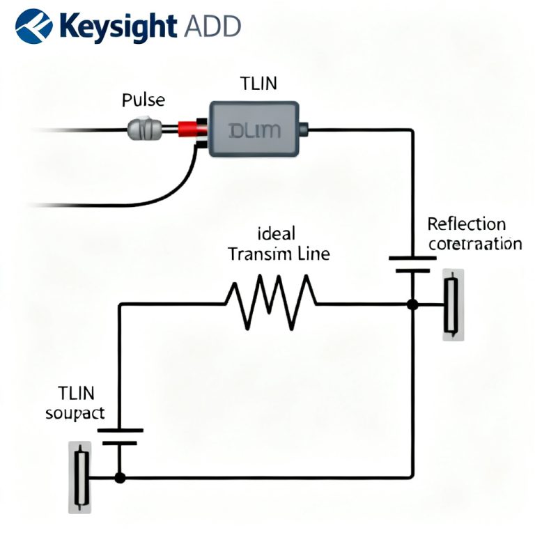
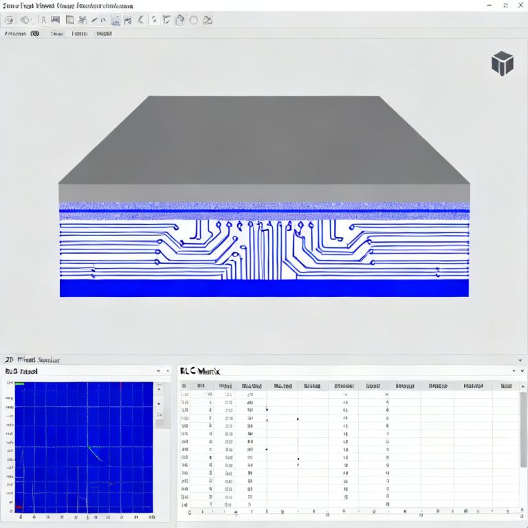
Accurate prediction of Crosstalk in High Speed PCB for DDR Interfaces requires 2D or 3D field solvers like Ansys HFSS or Cadence Sigrity. Extract S-parameters and simulate TDR profiles to identify impedance discontinuities. Key inputs include stackup materials, trace geometry, and edge rates.
Rule-of-Thumb Estimates
| Spacing | Estimated Crosstalk for High Speed PCB | Acceptability |
|---|---|---|
| 1W spacing | 10-15% | Unacceptable |
| 2W spacing | 4-6% | Marginal |
| 3W spacing | 1-2% | Acceptable |
These approximations vary based on stackup and edge rates. Always validate with simulation for production designs.
PCB Layout Strategies for Crosstalk Mitigation
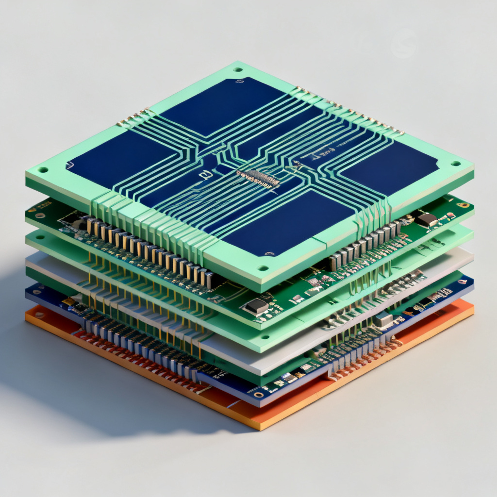
Stackup Design for High Speed PCB
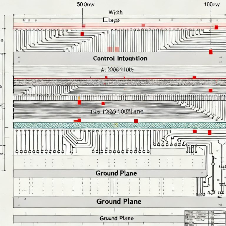
A proper stackup is the foundation for controlling Crosstalk in High Speed PCB for DDR Interfaces. Use stripline layers for critical buses, dedicate solid ground planes, and follow this 8-layer example: Layer 1 components, Layer 2 ground, Layer 3 address bus stripline, Layer 4 ground, Layer 5 power, Layer 6 data bus stripline, Layer 7 ground, Layer 8 bottom microstrip.
Trace Routing Rules
Implement spacing rules: 4W for address bus, 3W for data bus within byte lanes, and 5W between byte lanes with grounded guard traces. Match address traces within 100 mils and data traces within 10-20 mils. Minimize vias and use back-drilling for DDR4 and above.
Grounding and Return Paths
Ensure continuous return paths directly below signal traces. Use guard traces with vias every 1/10th wavelength for sensitive lines like DQS and CLK. Place stitching vias around board edges and connectors to maintain low-impedance return paths across layers.
Termination and Driver Selection
Enable On-Die Termination on both controller and DRAM to reduce reflections. Use the weakest driver strength meeting timing requirements to slow edge rates. For address buses, series resistors of 22-33 ohms dampen high-frequency ringing and reduce crosstalk.
Advanced Considerations for DDR4 and DDR5
DDR4 Fly-By Topology
DDR4 introduced fly-by topology for address/command buses, routing signals in a daisy-chain with short stubs under 500 mils. This reduces resonance and reflection that worsen Crosstalk in High Speed PCB for DDR Interfaces. Route the chain in a single direction without loops.
DDR5 Challenges
At data rates up to 8.4 Gbps, DDR5 requires Decision Feedback Equalization and on-die crosstalk cancellation. Use 5W spacing for address and 4W for data buses. Select low-loss materials like Megtron 6 or Rogers 4350B to manage dielectric loss at high frequencies.
Diagnostic Techniques for High Speed PCB
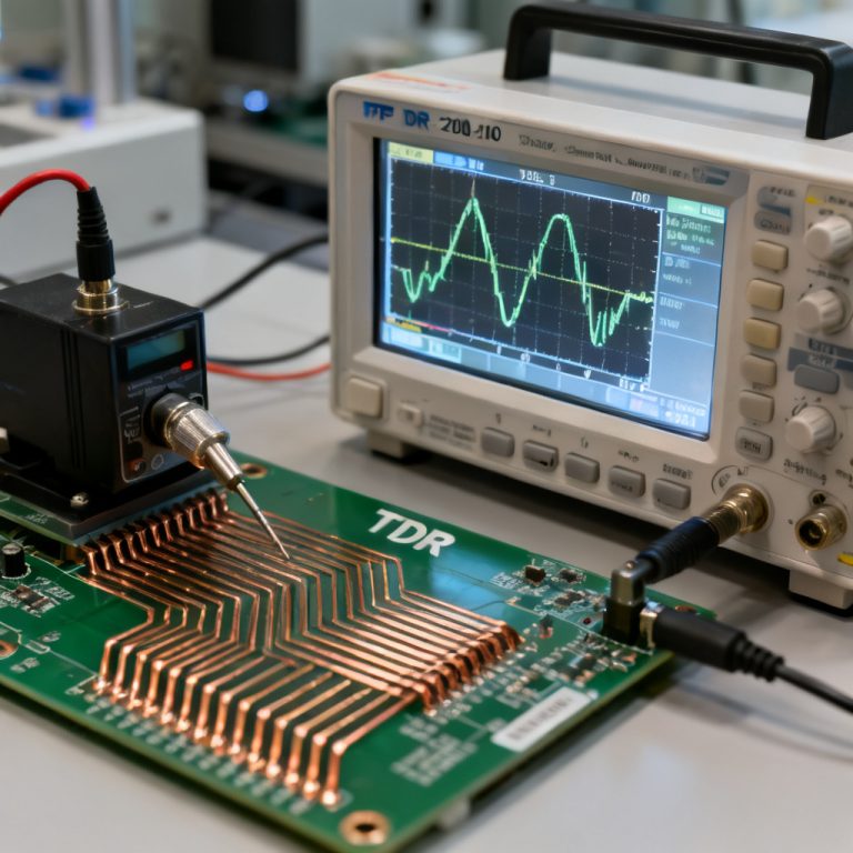
Time Domain Reflectometry
TDR reveals impedance profiles and identifies crosstalk locations. A dip indicates capacitive discontinuity; a spike indicates inductive discontinuity. Crosstalk appears as a broad dip or spike on the victim trace at the parallel coupling location.
Eye Diagram Analysis
Eye diagrams evaluate signal quality. Crosstalk in High Speed PCB for DDR Interfaces reduces vertical eye opening and closes horizontal timing margin. Deterministic jitter appears as a bimodal distribution on edges. Bathtub curves show increased bit error rates due to crosstalk.
Frequently Asked Questions
What is the primary cause of crosstalk in high speed PCB for DDR interfaces?
The primary cause is electromagnetic coupling between adjacent traces, driven by fast edge rates and long parallel routing lengths. Both address and data buses require specific mitigation strategies.
How does address bus crosstalk differ from data bus crosstalk?
Address bus crosstalk is dominated by multi-drop topology and stub effects, while data bus crosstalk involves bidirectional interference and simultaneous switching noise. Mitigation techniques differ accordingly.
What spacing is recommended for minimizing crosstalk in high speed PCB?
For address buses, use 4W to 5W spacing. For data buses within byte lanes, use 3W spacing. Between byte lanes, use 5W spacing with grounded guard traces for optimal performance.
Why is stripline preferred for DDR routing?
Stripline layers provide controlled impedance and eliminate far-end crosstalk by sandwiching traces between ground planes. This is essential for maintaining signal integrity in high-speed DDR designs.
What role does On-Die Termination play in crosstalk reduction?
ODT reduces reflections at the receiver, minimizing the energy available to couple onto adjacent traces. It is a standard feature in DDR3, DDR4, and DDR5 interfaces.