In high-speed PCB design, mastering decoupling capacitor selection and placement for power integrity PCB is critical to ensure stable voltage rails and minimize noise in your power distribution network. This guide consolidates industry best practices to help B2B engineers achieve reliable, high-performance designs.
The Physics of Decoupling – Understanding Power Integrity PCB
Power integrity PCB is fundamentally about maintaining a stable voltage across the power distribution network (PDN) under transient load conditions. The PDN impedance—from the VRM through the PCB planes, vias, and capacitors—must be kept low across a wide frequency range. Decoupling capacitor selection and placement for power integrity PCB directly influences this impedance profile.
The Role of Decoupling Capacitors in Power Integrity PCB
- Local Energy Storage: Capacitors supply instantaneous current during high-speed switching events, before the VRM can respond.
- Noise Bypass: They provide a low-impedance path for AC noise to return to ground, preventing it from coupling into other circuits.
- Resonance Damping: Properly selected capacitors dampen resonances between PCB planes, reducing ringing and radiated emissions.
Key Electrical Parameters for Power Integrity PCB
- Capacitance (C): Determines low-frequency storage. Larger values (e.g., 10 µF–100 µF) handle bulk decoupling at frequencies below ~1 MHz.
- Equivalent Series Resistance (ESR): Affects damping and heat dissipation. Low ESR (e.g., <10 mΩ for ceramic) is preferred for high-frequency performance, but too low can cause ringing with low-loss planes.
- Equivalent Series Inductance (ESL): The dominant factor for high-frequency decoupling. ESL limits the capacitor’s effectiveness above its self-resonant frequency (SRF). Lower ESL (e.g., 0.2 nH for 0402) extends useful bandwidth.
- Self-Resonant Frequency (SRF): The frequency at which the capacitor’s impedance is minimum (ESR limited). Above SRF, the capacitor behaves inductively. SRF is inversely proportional to the square root of (C × ESL). For high-speed designs, target SRF > 100 MHz.
The Impedance Target Approach in Power Integrity PCB
Designers define a target impedance (Z_target) for the PDN, typically calculated as (VDD × allowed ripple) / (transient current). For a 1.2 V rail with 5% ripple and 10 A transient, Z_target = (1.2 × 0.05) / 10 = 6 mΩ. The combined impedance of all decoupling capacitors for power integrity PCB must stay below this target from DC to the highest frequency of interest (e.g., 1 GHz).
Decoupling Capacitor Selection for Power Integrity PCB
Effective decoupling capacitor selection for power integrity PCB requires understanding capacitor technologies and their parasitics.
Capacitor Technologies Compared for Power Integrity PCB
- Multilayer Ceramic Capacitors (MLCCs): The workhorse for high-speed designs. They offer low ESL (0.2–0.5 nH for 0402/0201), low ESR, high SRF, and small footprints. X7R and X5R dielectrics are common; NP0/C0G provides better temperature stability but lower capacitance density.
- Tantalum Capacitors: Higher capacitance per volume but higher ESR and ESL. Suitable for bulk decoupling at low frequencies (e.g., <1 MHz) but avoid in high-speed paths due to voltage derating and failure risks.
- Aluminum Electrolytic: Very high capacitance but large ESL/ESR. Only for power input filtering, not for high-speed decoupling.
- Polymer Capacitors: Lower ESR than tantalum but still high ESL. Use sparingly for mid-frequency decoupling (1–10 MHz).
The “Capacitor Spreadsheet” Method (Bulk + Mid + High Frequency) for Power Integrity PCB
To cover a wide frequency range, use a mix of capacitor values, each targeting a specific frequency band:
- Bulk Decoupling (1–100 kHz): 10 µF–100 µF MLCCs (e.g., 0805 X7R). Place near VRM output.
- Mid-Frequency Decoupling (100 kHz–10 MHz): 0.1 µF–1 µF MLCCs (e.g., 0603 X7R). Place around IC power pins.
- High-Frequency Decoupling (10 MHz–1 GHz): 10 nF–100 nF MLCCs (e.g., 0402 or 0201 NP0). Place as close as possible to IC pins.

The “One-Value” Approach (Common Misconception) in Power Integrity PCB
Some designers use a single value (e.g., 0.1 µF) for all decoupling. This creates a narrow impedance trough and leaves gaps at lower frequencies. Modern high-speed designs require multiple values, typically 2–3 per voltage rail, spaced by a factor of 10–100 in capacitance.
Impact of Parasitics on Effective Capacitance in Power Integrity PCB
- DC Bias Effect: MLCC capacitance drops significantly with applied DC voltage (e.g., a 10 µF X7R may become 5 µF at 5 V). Always derate by 50–70% in high-voltage designs.
- Temperature Coefficient: X7R varies ±15% over -55°C to +125°C. NP0/C0G is stable but limited to ~1 nF in small packages.
- Aging: MLCCs lose capacitance over time (up to 5% per decade). Account for worst-case tolerance.
Practical Selection Example for a 1.0 V Core Rail in Power Integrity PCB
- Target impedance: 5 mΩ up to 500 MHz
- Capacitor mix:
- 10 × 100 µF (0805, X7R) – bulk
- 10 × 1 µF (0603, X7R) – mid
- 20 × 0.1 µF (0402, NP0) – high
- 20 × 10 nF (0201, NP0) – ultra-high
- Total ESL: ~0.2 nH per 0402, ~0.5 nH per 0603 – ensure combined impedance < 5 mΩ.
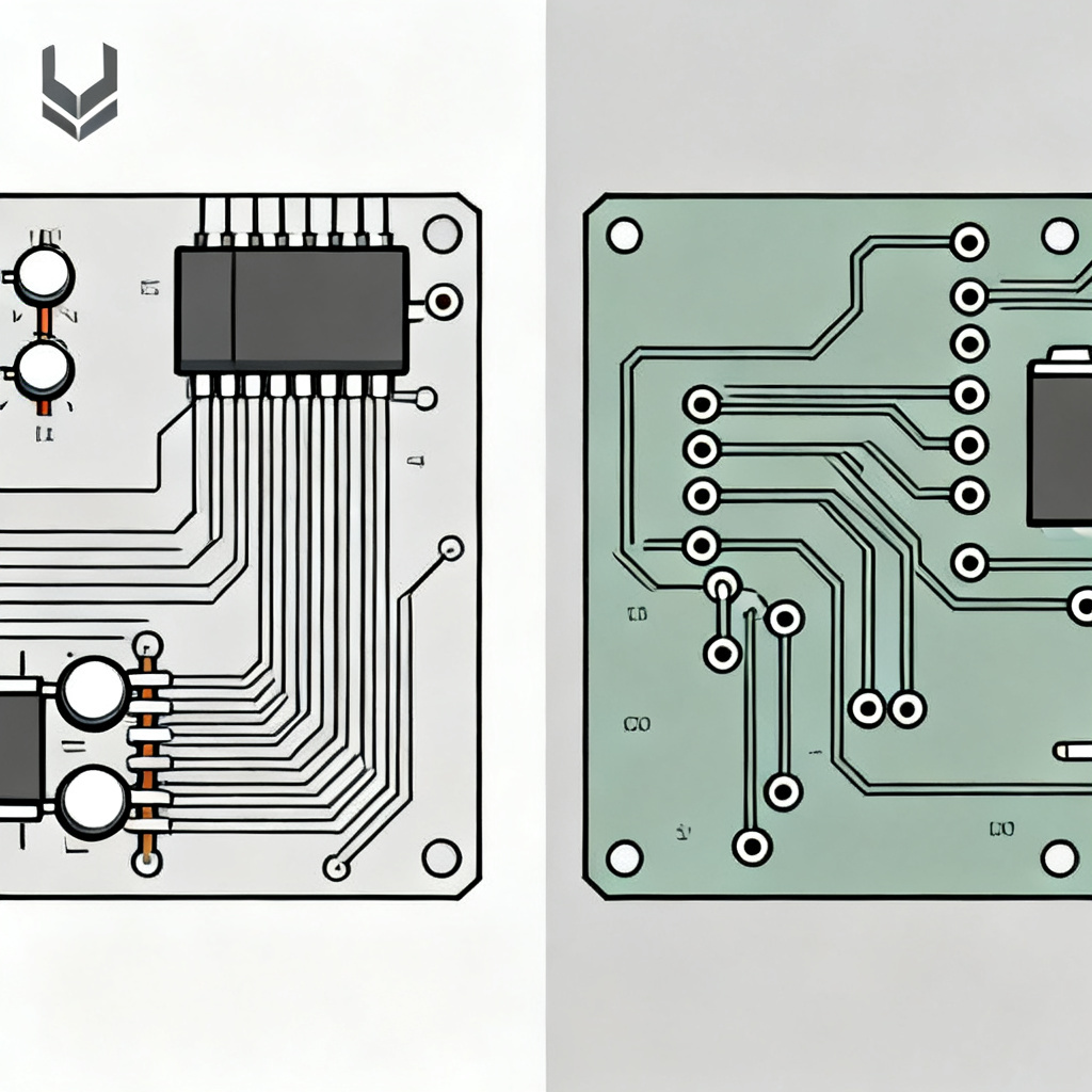
Placement and Mounting Inductance for Power Integrity PCB
Optimal decoupling capacitor placement for power integrity PCB minimizes loop inductance, which is critical for high-frequency performance.
The Loop Inductance Problem in Power Integrity PCB
The effective inductance of a decoupling capacitor is not just its package ESL. The total loop inductance includes:
- Capacitor body ESL
- Solder pad and via inductance
- Trace inductance from pad to via to plane
- Via inductance through the PCB stackup
Rule of Thumb: Every 1 mm of trace length adds ~1 nH of inductance. A 0.5 mm via adds ~0.3 nH. Total loop inductance can easily exceed 5 nH, limiting high-frequency performance.
Optimal Placement Rules for Power Integrity PCB
- Minimize Distance: Place capacitors within 1–2 mm of the IC power pins. For BGA packages, use capacitors on the bottom side directly under the BGA.
- Use Short, Wide Traces: Connect capacitor pads to vias with the widest possible trace (e.g., 0.5 mm or wider). Avoid long, narrow traces.
- Via Placement: Place vias as close as possible to capacitor pads—ideally within 0.5 mm. Use multiple vias per capacitor (e.g., 2 vias for each pad) to reduce inductance.
- Symmetry: For differential pairs or clock lines, place identical capacitors symmetrically to maintain signal integrity.
Orientation and Stitching for Power Integrity PCB
- Capacitor Orientation: Rotate capacitors so that the current path from the pad to the via is as short as possible. For 0402, place vias at the ends of the pads.
- Ground Plane Stitching: Connect capacitor ground pads directly to the ground plane with multiple vias. Avoid “daisy-chaining” capacitors through traces.
The “Flip-Chip” and “Embedded” Strategies for Power Integrity PCB
- Flip-Chip Mounting: Mount capacitors on the IC substrate itself (e.g., in-package decoupling). This reduces loop inductance to <0.1 nH but adds cost.
- Embedded Capacitors: Buried capacitance layers (e.g., 1–10 nF per square inch) in the PCB substrate provide ultra-low inductance (<0.01 nH). Ideal for very high-speed designs (>10 Gbps).
Placement for Different IC Types in Power Integrity PCB
- FPGAs and ASICs: Use a “capacitor farm” around the BGA with 20–50 capacitors per power rail. Place them in a ring pattern, alternating between VDD and GND vias.
- DDR Memory: Place capacitors near each DDR chip and along the VTT rail. Use 0402 or 0201 for high-frequency decoupling.
- Power Regulators: Place bulk capacitors at the regulator output, then distribute mid- and high-frequency capacitors near the load.
Advanced Techniques – Simulation and Optimization for Power Integrity PCB
Advanced simulation ensures that decoupling capacitor selection and placement for power integrity PCB meets target impedance across all frequencies.
PDN Simulation Tools for Power Integrity PCB
- SPICE Models: Use RLC models for capacitors and vias. Simulate the PDN impedance vs. frequency.
- 3D EM Solvers: Tools like Ansys SIwave or CST simulate full-wave effects including plane resonances.
- Impedance Profiles: Plot Z(f) to identify peaks. Add capacitors to dampen peaks below Z_target.

Anti-Resonance Avoidance in Power Integrity PCB
When multiple capacitor values are used, their SRFs create anti-resonance peaks (parallel resonance) where impedance spikes. To mitigate:
- Use capacitors with different ESR values (e.g., mix low-ESR MLCCs with slightly higher-ESR types).
- Ensure the SRF of the smallest capacitor is > the highest frequency of interest.
- Simulate the combined impedance to verify no peak exceeds Z_target.
Temperature and Aging Compensation for Power Integrity PCB
- Derate capacitance by 20–30% for X7R at operating temperature.
- Use NP0/C0G for critical high-frequency paths where stability is paramount.
Cost vs. Performance Trade-offs in Power Integrity PCB
- 0201 capacitors offer lower ESL but are more expensive and harder to assemble.
- 0402 is the sweet spot for high-speed designs (cost + performance).
- For mid-frequency, 0603 X7R is cost-effective.
Common Mistakes and How to Avoid Them in Power Integrity PCB
Avoid these pitfalls to ensure successful decoupling capacitor selection and placement for power integrity PCB:
| Common Mistake in Power Integrity PCB | Consequence | Solution |
|---|---|---|
| Using only 0.1 µF caps | Narrow impedance coverage | Use 2–3 values per rail |
| Long traces to capacitors | High loop inductance | Place caps within 1 mm of IC |
| Single via per pad | Inductance bottleneck | Use 2+ vias per pad |
| Ignoring DC bias effect | Capacitance drop | Derate by 50% for X7R |
| Daisy-chaining caps | Increased inductance | Connect each cap directly to planes |
| Mixing capacitor types without simulation | Anti-resonance peaks | Simulate combined impedance |
Real-World Implementation Checklist for Power Integrity PCB
Follow this checklist for effective decoupling capacitor selection and placement for power integrity PCB:
- Define Z_target from voltage ripple and transient current specs.
- Select capacitor mix (bulk, mid, high) based on frequency range.
- Choose package sizes (0402/0201 for high-speed, 0603/0805 for bulk).
- Place capacitors within 1 mm of IC pins, using short wide traces and multiple vias.
- Simulate PDN impedance with SPICE or EM tools.
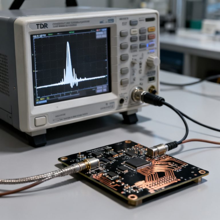
- Verify with measurements using a VNA or impedance analyzer.
- Document and iterate for next revision.
For high-speed PCB designs, our services provide controlled impedance and embedded capacitance options to simplify your work.
FAQ: Decoupling Capacitor Selection and Placement for Power Integrity PCB
What is the most important factor in decoupling capacitor selection for power integrity PCB?
The most important factor is minimizing equivalent series inductance (ESL) to ensure effective high-frequency decoupling. Lower ESL capacitors, such as 0402 MLCCs, are preferred for decoupling capacitor selection for power integrity PCB.
How does placement affect decoupling capacitor performance for power integrity PCB?
Placement directly impacts loop inductance. Capacitors placed within 1–2 mm of IC power pins with short, wide traces and multiple vias achieve optimal decoupling capacitor placement for power integrity PCB.
What is the target impedance in power integrity PCB design?
Target impedance is the maximum allowable PDN impedance, calculated as (VDD × allowed ripple) / (transient current). It guides decoupling capacitor selection and placement for power integrity PCB to ensure stable voltage rails.
Why should I avoid using only 0.1 µF capacitors for decoupling in power integrity PCB?
Using a single value creates narrow impedance coverage and leaves gaps at lower frequencies. A mix of capacitor values (bulk, mid, high) is essential for comprehensive decoupling capacitor selection for power integrity PCB.
What is the role of ESR in decoupling capacitors for power integrity PCB?
ESR affects damping and heat dissipation. Low ESR is preferred for high-frequency performance, but too low ESR can cause ringing. Balancing ESR is part of effective decoupling capacitor selection and placement for power integrity PCB.