[rank_math_breadcrumb]
In high-speed PCB design, differential pair impedance is the backbone of reliable data transmission. Protocols like USB, HDMI, PCIe, and Gigabit Ethernet rely on controlled differential impedance—typically 100Ω or 90Ω—to maintain signal integrity. This article compares edge-coupled vs broadside-coupled topologies to help you choose the best approach for your next high-speed board.
The Fundamentals of Differential Pair Impedance
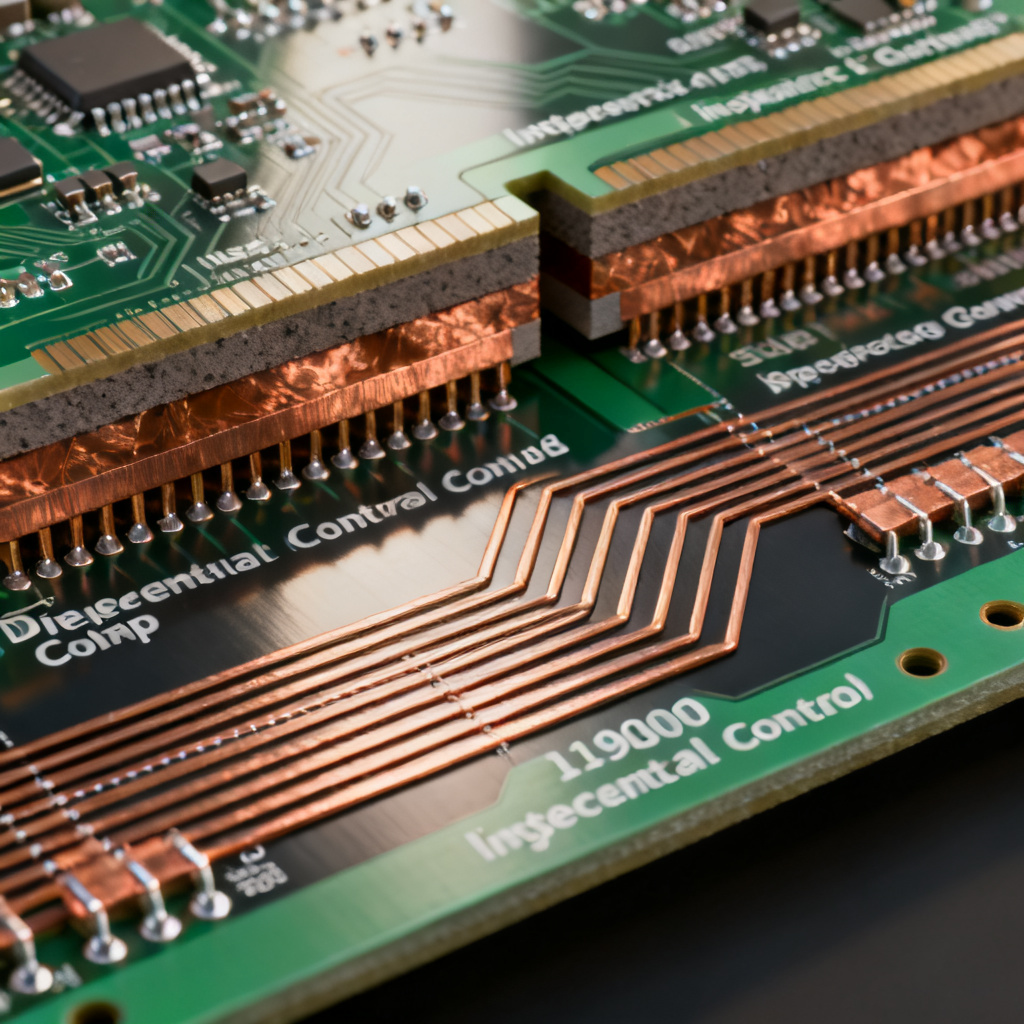
A differential pair consists of two traces carrying equal but opposite signals. The differential pair impedance (Zdiff) is a function of trace width (W), thickness (T), dielectric height (H) to the reference plane, dielectric constant (Dk), and spacing (S) between traces. Both edge-coupled and broadside-coupled topologies achieve the target Zdiff (typically 100Ω) through different geometric relationships.
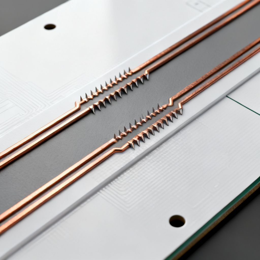
Edge-Coupled Differential Pairs (Side-by-Side)
What is an Edge-Coupled Pair?
An edge-coupled differential pair routes two traces on the same layer, separated by a specific gap (S), referenced to a single ground plane below. This is the most common method for differential pair impedance control in standard PCB designs.
Key Characteristics
Impedance control: Zdiff is primarily controlled by spacing (S) and height (H) to the reference plane. As S decreases, coupling increases, lowering Zdiff. Manufacturing simplicity: Requires only one layer, making it easy to design, inspect, and fabricate. Crosstalk and noise: Excellent common-mode rejection due to close proximity to the ground plane, minimizing loop area and radiated emissions. Limitations: Requires significant board space for trace width and spacing; tight spacing can cause etching variations and increased insertion loss.
Real-World Application
Ideal for most high-speed designs where space is not extremely tight, commonly used in 4-layer to 8-layer boards for protocols like USB 3.0 and HDMI.
Broadside-Coupled Differential Pairs (Stacked)
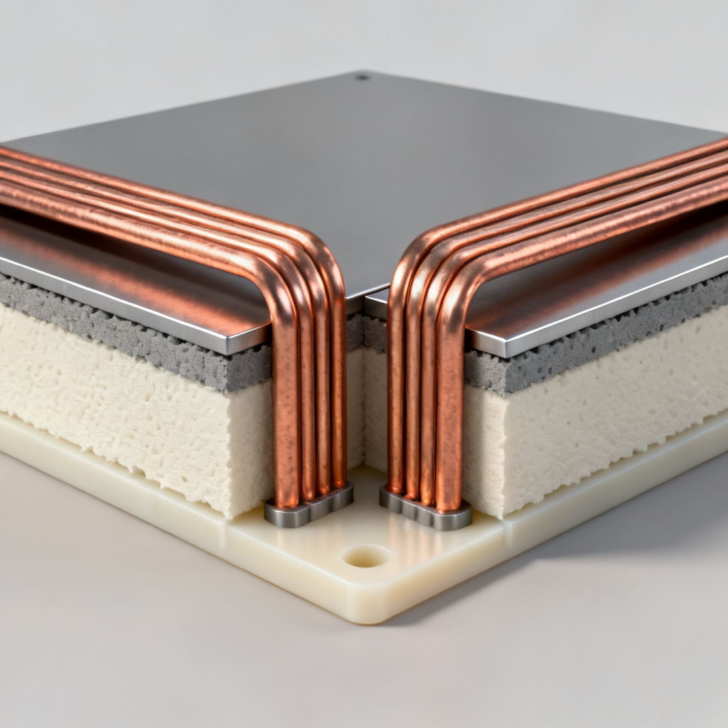
What is a Broadside-Coupled Pair?
Per differential pair routing rules, a broadside-coupled differential pair places two traces on adjacent layers, directly above each other, referenced to ground planes above and below. This creates vertical coupling, allowing for narrower trace widths to achieve the same differential pair impedance.
Key Characteristics
Impedance control: Zdiff is controlled by vertical separation (dielectric thickness between layers) and trace width. Stronger coupling than edge-coupled, enabling space savings. Manufacturing complexity: Requires precise layer-to-layer registration; misalignment shifts impedance, adding cost and stricter tolerances. Signal integrity advantages: Lower insertion loss due to narrower traces, better skew control, and reduced radiated emissions due to confined fields. Limitations: Increases layer count, is extremely sensitive to dielectric thickness variations, and via stubs can be problematic at very high frequencies.
Real-World Application
Used in ultra-high-speed designs (25+ Gbps SerDes) where signal integrity is paramount and board space is at a premium, such as in 16+ layer backplanes and mobile devices.
Head-to-Head Comparison: Which Is Better for Your High-Speed PCB?
Based on synthesis of authoritative sources, here is a direct comparison across critical parameters for differential pair impedance control.
| Parameter | Edge-Coupled | Broadside-Coupled | Winner (for most cases) |
|---|---|---|---|
| Space Efficiency | Poor. Requires wider traces and larger gaps. | Excellent. Uses narrower traces, saving routing channels. | Broadside |
| Manufacturing Cost | Low. Standard processes, no special alignment. | High. Requires tight layer-to-layer registration. | Edge |
| Impedance Tolerance | Moderate. Sensitive to etch and dielectric height. | Very sensitive to layer alignment and dielectric thickness. | Edge (more robust) |
| Insertion Loss | Higher due to wider traces (skin effect). | Lower due to narrower traces. | Broadside |
| Crosstalk Immunity | Good. Close to ground plane. | Excellent. Fields are vertically confined. | Broadside |
| Skew Control | Moderate. Subject to Dk variations across layer. | Better. Traces are vertically close. | Broadside |
| Ease of Debug/Probe | Easy. Both traces on same layer. | Difficult. Traces on different layers. | Edge |
| Common-Mode Noise | Good rejection due to ground plane reference. | Excellent due to symmetric stackup. | Broadside |
The Verdict
There is no single “better” topology. Choose edge-coupled when cost is primary, board space is available, data rates are below 10-15 Gbps, and easy testing is needed. Choose broadside-coupled for ultra-high-speed (25+ Gbps), tight board space, lowest insertion loss, and when working with a high-precision manufacturer.
Practical Design Considerations for B2B PCB Manufacturing

Stackup is King
For broadside coupling, the dielectric between differential layers (thin prepreg like 1080) must have tightly controlled thickness and Dk. For edge-coupled, ensure continuous reference planes.
Impedance Modeling
Use 2D field solvers like Polar Si9000 or Simbeor to model differential pair impedance for your exact stackup. Model both options to see resulting trace widths and gaps.
Manufacturing Tolerances
Communicate impedance requirements clearly. For broadside, specify layer-to-layer registration tolerance (e.g., ±0.1mm). For edge-coupled, specify trace width/spacing tolerance (e.g., ±10%). Our factory achieves ±0.05mm registration for high-precision broadside designs.
Via Design and Material Selection
Transitions between layers require careful via design with back-drilling to remove stubs at high frequencies. Choose low-loss materials (Rogers 4350B, Isola FR408HR, Megtron 6) for frequencies above 10 GHz.
Frequently Asked Questions
What is the main difference between edge-coupled and broadside-coupled differential pair impedance?
Edge-coupled routes traces side-by-side on the same layer, while broadside-coupled stacks them on adjacent layers. Broadside offers better space efficiency and lower loss but requires tighter manufacturing tolerances for differential pair impedance control.
Which topology is better for 100 Ohm differential pair impedance?
Both can achieve 100Ω differential pair impedance. Edge-coupled is simpler and more cost-effective for most designs, while broadside-coupled is preferred for ultra-high-speed applications requiring minimal loss.
How does manufacturing tolerance affect differential pair impedance in broadside-coupled designs?
Layer-to-layer misalignment can shift Zdiff significantly, requiring precise registration (e.g., ±0.1mm) and careful stackup design to maintain target differential pair impedance.
Can I mix edge-coupled and broadside-coupled pairs on the same PCB?
Yes, but transitions must be carefully designed with impedance-matched vias and back-drilling to avoid signal integrity issues at high frequencies.
What is the typical differential pair impedance for PCIe 5.0?
PCIe 5.0 typically requires 85Ω or 100Ω differential pair impedance, depending on the standard. Both edge-coupled and broadside-coupled topologies can meet this requirement with proper stackup design.