[rank_math_breadcrumb]
In high-speed PCB design, BGA breakout regions often compromise differential pair impedance, causing signal reflection and jitter. This page explains why these impedance discontinuities occur and provides proven fixes—including anti-pad optimization, via backdrilling, and trace geometry tuning—to maintain 100Ω or 90Ω control for reliable high-speed performance.
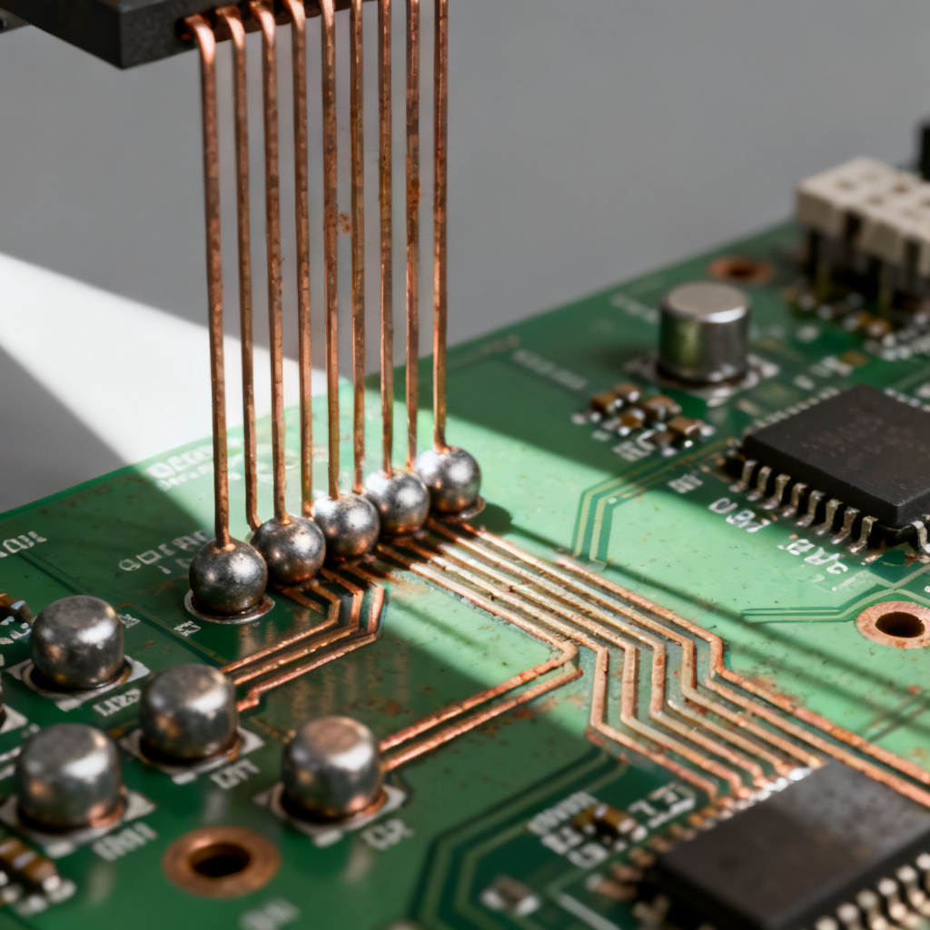
Why BGA Breakout Regions Compromise Differential Pair Impedance
1.1 The Fundamental Geometry Discontinuity
Inside a BGA footprint, differential pair impedance faces its first challenge: traces must neck down to fit between solder balls. A typical 0.8mm pitch BGA leaves only 0.15mm to 0.2mm of available routing channel between adjacent balls. This forces designers to reduce trace width from the target 6-8 mils (for 100Ω differential impedance) down to 3-4 mils. According to leading signal integrity analysis, this width reduction alone increases the characteristic impedance by 15-25% because the trace-to-ground plane capacitance decreases faster than the inductance drops.
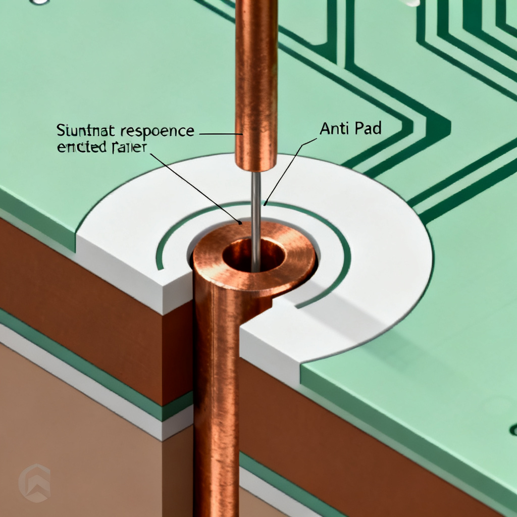
1.2 Via Stub and Anti-Pad Effects
When differential pairs transition from the top layer to inner layers through BGA vias, two additional impedance disruptors appear:
Via Stub Resonance: The unused portion of a via barrel (the stub) acts as a quarter-wave resonator. At frequencies where the stub length equals λ/4, it creates a short circuit that reflects energy back into the signal path. For a 20-mil stub in FR4, this resonance occurs around 15GHz—well within the operating range of modern high-speed interfaces.
Anti-Pad Coupling: The anti-pad (clearance hole in the ground plane around each via) creates a local region of reduced capacitance. When two differential vias have anti-pads that are too large or asymmetrically shaped, the odd-mode impedance increases while common-mode impedance decreases, breaking the differential pair’s inherent balance.
1.3 Layer Transition and Reference Plane Discontinuity
Most BGA breakouts require routing on the top layer, then dropping to inner layers via microvias or through-hole vias. The reference plane for the differential pair changes from the top copper pour to an inner ground layer. If the via transition lacks a proper return path—such as a ground via placed within 20 mils of each signal via—the current return path must find an alternative route through the BGA ball field, creating a large inductive loop that spikes impedance.
1.4 Ball Field Capacitance Loading
The BGA solder balls themselves, along with the landing pads on the PCB, add parasitic capacitance to the transmission line. Each ball pad can add 0.1-0.3pF of capacitance. When multiple differential pairs are routed through the same ball field, the cumulative loading can reduce the local impedance by 5-10Ω. This is especially problematic in dense BGA packages where the ball field extends 10-15 rows deep.
How to Fix BGA Breakout Impedance Discontinuities
2.1 Optimize Anti-Pad Geometry
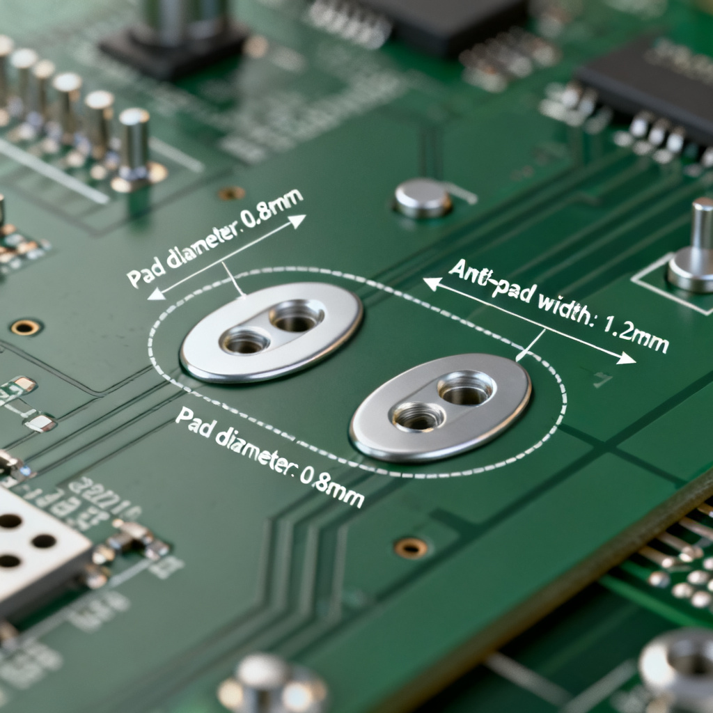
The most effective single fix is anti-pad tuning. For differential pair vias, use elliptical or slotted anti-pads rather than circular ones. The long axis of the ellipse should align with the differential pair direction. This creates a controlled impedance transition zone.
Implementation Guide:
- For 100Ω differential pairs in 0.8mm pitch BGA: use anti-pads with 12-mil width and 28-mil length
- Maintain a 1:2 to 1:3 aspect ratio between the short and long axes
- Ensure the anti-pad gap between the two signal vias is 8-10 mils wider than the via diameter
Why it works: The elliptical shape increases the clearance around each via in the direction of signal propagation, reducing capacitive loading while maintaining ground plane continuity perpendicular to the pair. This balances the odd-mode and even-mode impedances.
2.2 Implement Backdrilling for Via Stub Elimination
Backdrilling removes the unused via barrel stub from the bottom of the PCB, eliminating the quarter-wave resonance. For BGA breakouts, backdrill from the bottom side to within 10 mils of the signal layer.
Critical Parameters:
- Backdrill bit diameter: 20-25 mils (must be larger than the via pad)
- Target stub length: <10 mils for frequencies up to 28Gbps
- For multilayer boards: backdrill only vias carrying differential signals, not ground vias
Alternative: Use Buried or Blind Vias in HDI designs. A stacked microvia structure (via-in-pad with sequential lamination) eliminates stubs entirely but increases cost by 30-50%. For most B2B applications, backdrilling offers the best cost-performance balance.
2.3 Trace Width and Spacing Compensation in the Breakout Zone
To maintain constant differential impedance through the necked-down region, apply these geometry rules:
For the breakout region (between BGA balls):
- Reduce trace width to 3.5-4 mils (from 6 mils in main routing)
- Increase trace spacing to 8-10 mils (from 6 mils in main routing)
- Use a 45-degree taper over 50-100 mils to transition between widths
Impedance Calculation Check: For a 4-layer stackup with 4-mil core and 1oz copper:
- Main routing: 6-mil width, 6-mil spacing → 100Ω differential
- Breakout: 3.5-mil width, 9-mil spacing → 100Ω differential (verified with 2D field solver)
Why spacing increases help: As traces narrow, the mutual inductance between the two traces increases. Widening the spacing reduces this inductive coupling, keeping the differential impedance stable.
2.4 Add Ground Via Fences for Return Path Continuity
Place ground vias adjacent to each differential via pair within the BGA field. The rule of thumb is: one ground via per two signal vias, placed no more than 25 mils away.
Optimal Layout:
- For every differential pair breakout, place a ground via on each side of the pair
- Connect these ground vias to the inner ground plane with a thermal spoke pattern to prevent solder wicking during assembly
- In dense BGA designs, use via-in-pad for ground vias to save space
Signal Integrity Benefit: Ground vias reduce the return current loop area by 60-80%, lowering the effective inductance and maintaining impedance within 5% of target.
2.5 Use Non-Functional Pad Removal
In the BGA breakout region, remove non-functional pads (pads on inner layers not connected to any trace) from signal vias. These pads add parasitic capacitance that lowers impedance.
Implementation:
- For inner layers 2 through N-1, remove all pads from signal vias except the pad on the layer where the trace connects
- Keep the anti-pad clearance on all layers to maintain consistent capacitance
- Use a “padless via” design rule in your PCB layout tool (e.g., Altium’s “Remove Pads” option)
2.6 Layer Stackup Optimization
Choose a stackup that minimizes impedance variation during layer transitions:
Recommended for High-Speed BGA Breakout (6-layer example):
| Layer | Function | Differential Pair Impedance Control Notes |
|---|---|---|
| Layer 1 (Top) | Signal + BGA pads | Thin prepreg (3-4 mils) to ground plane |
| Layer 2 | Ground plane | Solid, no splits |
| Layer 3 | Power plane | With anti-pads for vias |
| Layer 4 | Signal | Secondary routing |
| Layer 5 | Ground plane | Solid |
| Layer 6 | Bottom | Component |
Key Requirement: The distance between Layer 1 and Layer 2 (prepreg thickness) should be 3-4 mils. A thinner dielectric reduces the impedance change when traces neck down because the reference plane is closer, increasing capacitance.
2.7 Simulation and Validation
Before finalizing the design, run 3D electromagnetic simulation of the entire BGA breakout region:
- Extract S-parameters from the BGA ball to the first via transition
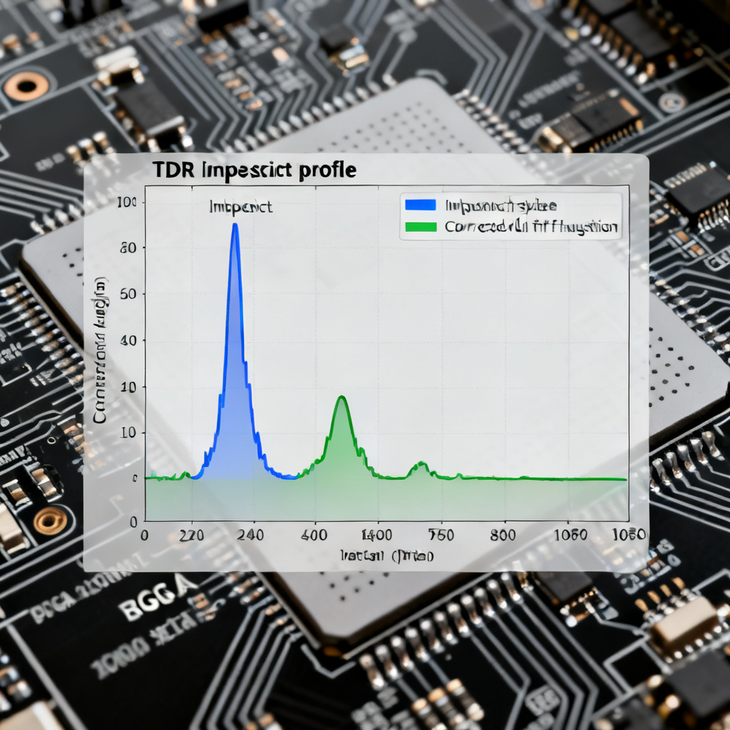
- Check TDR impedance profile for any dips or peaks exceeding ±10% of target
- Validate eye diagram at the operating data rate (e.g., 25Gbps NRZ)
Tools: Use Ansys HFSS, CST Microwave Studio, or Keysight ADS for accurate modeling. For quick checks, open-source tools like OpenEMS can work but require more setup time.
Acceptance Criteria:
- Impedance variation: < ±10% across the breakout region
- Insertion loss: < 0.5dB at Nyquist frequency
- Return loss: > 15dB up to 20GHz
Practical Design Rules for BGA Breakout Impedance Control
3.1 Rule 1: Start with the BGA Footprint
- Use solder-mask-defined (SMD) pads for BGA balls, not non-solder-mask-defined (NSMD). SMD pads provide more consistent capacitance.
- Keep the pad diameter to 12 mils for 0.8mm pitch BGA (ball diameter typically 16 mils).
- Avoid placing differential pairs through the center of the BGA field where ball density is highest. Route pairs near the perimeter when possible.
3.2 Rule 2: Limit Breakout Length
The necked-down region should not exceed 200 mils total (from BGA ball to first via). Longer breakouts increase cumulative impedance mismatch and crosstalk.
3.3 Rule 3: Use Differential Pair Symmetry
Both traces in a differential pair must have identical breakout geometry:
- Same number of vias
- Same via structure (microvia vs. through-hole)
- Same length of necked-down region
Asymmetry introduces skew (time delay difference) that converts common-mode noise to differential noise.
3.4 Rule 4: Avoid 90-Degree Bends
In the breakout region, use only 45-degree or arc-based bends. A 90-degree bend creates a 0.5-1Ω impedance bump due to the increased trace width at the corner. Use mitered bends with a 1:1.5 ratio for best performance.
Case Study: Fixing a 25Gbps BGA Breakout
Problem: A 0.8mm pitch BGA carrying 4 differential pairs at 25Gbps showed 15dB return loss at 12.5GHz (Nyquist frequency). TDR revealed a 12Ω impedance spike (from 100Ω to 112Ω) in the breakout region.
Root Cause Analysis:
- Circular anti-pads (16-mil diameter) were used
- No ground vias adjacent to signal vias
- Trace width reduced to 3 mils without spacing adjustment
Fix Applied:
- Changed anti-pads to elliptical (12×28 mils)
- Added ground vias 20 mils from each signal via
- Adjusted breakout trace width to 4 mils and spacing to 9 mils
- Backdrilled vias to remove 15-mil stubs
Result:
- Return loss improved to 22dB at 12.5GHz
- Impedance variation reduced to ±3% (97-103Ω)
- Eye opening increased from 45% to 78% of unit interval
FAQ: BGA Breakout Regions and Differential Pair Impedance
What is the main cause of impedance discontinuity in BGA breakout regions?
The primary cause is the forced reduction in trace width to fit between BGA balls, combined with via stubs, anti-pad coupling, and layer transitions that disrupt the controlled differential pair impedance.
How can I fix via stub resonance in BGA breakouts?
Backdrilling is the most effective method. Remove the unused via barrel stub to within 10 mils of the signal layer. For HDI designs, blind or buried vias can eliminate stubs entirely.
What is the recommended anti-pad shape for differential vias?
Use elliptical or slotted anti-pads with a 1:2 to 1:3 aspect ratio. The long axis should align with the differential pair direction to balance capacitive loading and maintain impedance control.
Why do ground vias help in BGA breakout impedance control?
Ground vias provide a continuous return path for the differential signal, reducing the inductive loop area. This minimizes impedance spikes and maintains signal integrity, especially during layer transitions.
What are the key design rules for maintaining differential pair impedance in BGA breakouts?
Key rules include: using SMD pads, limiting breakout length to 200 mils, ensuring trace symmetry, avoiding 90-degree bends, and compensating trace width and spacing to match target impedance (e.g., 100Ω or 90Ω).