[rank_math_breadcrumb]
In high speed PCB design, mastering differential vs common mode radiation in EMI EMC high speed PCB design is essential for signal integrity and regulatory compliance. This pillar page explains the physics, differences, and mitigation strategies for both radiation types.
Understanding Differential Mode Radiation in EMI EMC High Speed PCB Design
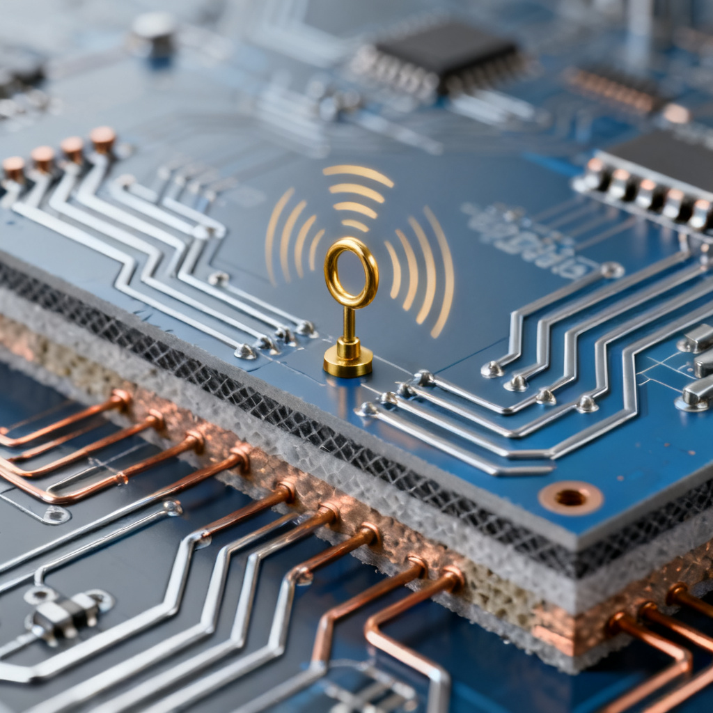
Differential mode radiation in EMI EMC high speed PCB design originates from the intended signal current loop. It is the predictable, designed current path that must be carefully managed.
Physics of Differential Mode Radiation
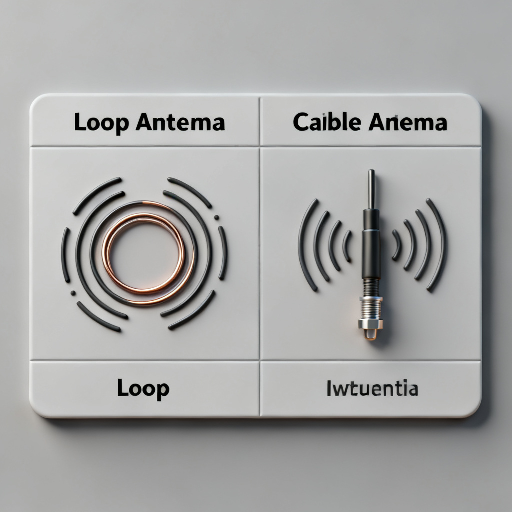
Current flows out on the signal trace and returns through the ground plane. The loop area formed by this path acts as a small loop antenna. The electric field from differential mode radiation is proportional to current amplitude, loop area, and the square of frequency. Near-field measurements show a dominant magnetic field component.
Key Characteristics
Differential mode radiation is predictable and can be modeled using SPICE or field solvers. It has low radiation impedance and is directly related to your circuit layout.
Control Techniques for Differential Mode Radiation
- Minimize loop area: Place the return path directly under the signal trace. For microstrip, keep trace width and dielectric height minimal.
- Use solid ground planes: An uninterrupted ground plane below the signal layer collapses the loop area effectively.
- Route differential pairs tightly: For high-speed differential signals, keep the pair closely coupled so return current flows in the adjacent trace.
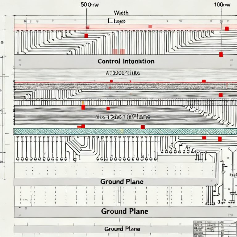
- Optimize layer stackup: Use stripline configuration (signal between two ground planes) to contain fields and reduce radiation by up to 30 dB.
Understanding Common Mode Radiation in EMI EMC High Speed PCB Design
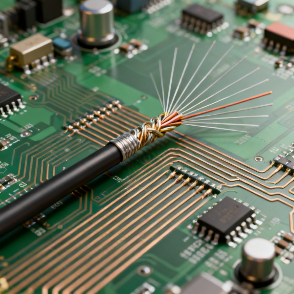
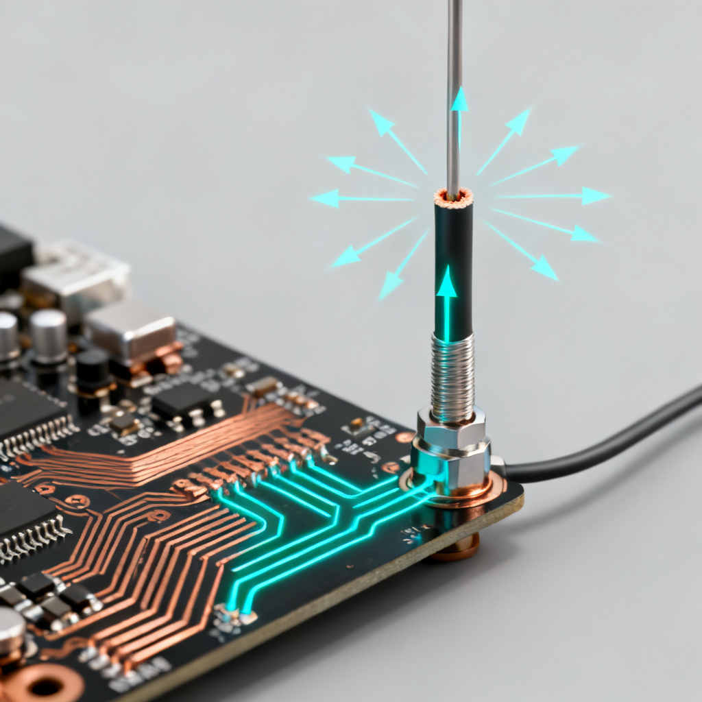
Common mode radiation is the most challenging aspect of EMI EMC high speed PCB design. It is caused by parasitic currents flowing in the same direction on all conductors, including signal and ground paths.
Physics of Common Mode Radiation
Unwanted current flows from the signal trace through the load and returns through the entire system ground, including cables and chassis. The entire cable or system chassis acts as a monopole or dipole antenna. Common mode radiation is almost always caused by ground bounce, power supply noise, or skew in differential pairs. The electric field is proportional to common mode current, cable length, and frequency. Even microamps of common mode current can violate FCC limits at high frequencies because cable length can be very large.
Key Characteristics
Common mode radiation is unpredictable and difficult to simulate without a full 3D EM model including cables. It has high radiation impedance and shows a dominant electric field in near-field measurements. I/O cables are the most common source of common mode radiation.
Control Techniques for Common Mode Radiation
- Eliminate ground bounce: Use decoupling capacitors (0.1 µF and 1 nF) directly at IC power pins. Use a dedicated power plane adjacent to the ground plane to create distributed capacitance.
- Control skew in differential pairs: Keep trace length matching within 5 mils for high-speed interfaces. Use serpentine routing and precise differential termination resistors.
- Apply filtering at I/O ports: Use common mode chokes (CMC) at connectors, ferrite beads on power lines, and shielded connectors bonded to chassis ground.
- Use via stitching: Place ground vias along board edges every 1/10th of a wavelength to create a Faraday cage. Use guard traces stitched to ground every 100 mils.
Differential vs Common Mode Comparison for EMI EMC High Speed PCB Design
| Feature | Differential Mode (DM) | Common Mode (CM) |
|---|---|---|
| Source | Intended signal current loop | Parasitic, unintended currents |
| Current Direction | Equal and opposite on trace & return | Same direction on all conductors |
| Antenna Type | Small loop antenna | Large cable/monopole antenna |
| Emission Level | Proportional to loop area | Proportional to cable length |
| Frequency Dependence | f² (very high roll-off) | f (linear roll-off) |
| Predictability | High (simulatable) | Low (hard to model) |
| Mitigation | Minimize loop area, use ground planes | Filtering, grounding, skew control |
Case Study: Common Mode Failure in High Speed PCB Design
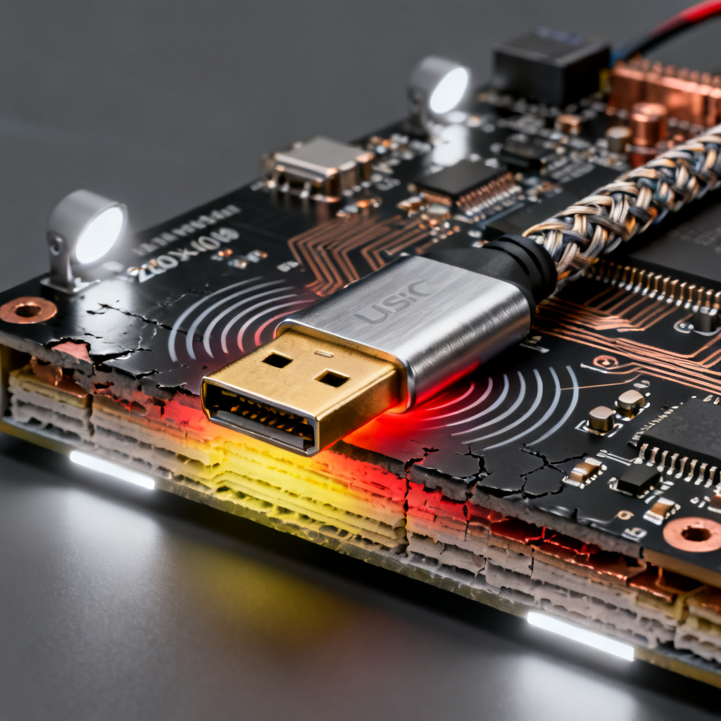
A high-speed digital board passed all signal integrity tests but failed FCC Class B radiated emissions at 200 MHz. The failure at 200 MHz suggested a harmonic of the 100 MHz clock. Near-field probing showed a strong E-field at the USB connector. The root cause was a 20-mil length mismatch in the differential USB pair, creating a small common mode current. The USB cable acted as a 1-meter antenna radiating at the 2nd harmonic. The solution involved redesigning the USB pair for zero skew, adding a common mode choke at the connector, and connecting the USB connector shell directly to chassis ground with a wide copper strap. Emissions dropped by 15 dB, passing the test.
Design Rules for Your High Speed PCB from Our B2B Manufacturing Perspective
As your manufacturing partner, we enforce these rules for first-pass EMC success in high speed PCB design:
- Layer stack: Use 6+ layers with Signal-Ground-Power-Signal-Ground configuration.
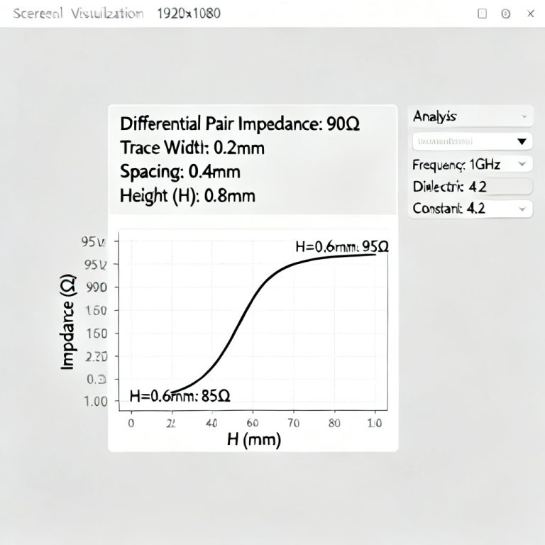
- Differential pairs: Maintain 100-Ohm impedance with length matching to ±5 mils.
- Decoupling: Place one capacitor per power pin plus bulk capacitors.
- I/O filtering: Mandatory common mode chokes on all external cables.
- Grounding: Single-point ground for analog, multi-point ground for digital. Never split the ground plane under a high-speed trace.