[rank_math_breadcrumb]
In high-speed PCB design, dielectric height (H) changes differential pair impedance more than any other variable. Understanding this sensitivity is critical for achieving 100 Ohm or 90 Ohm impedance targets in your custom high-speed PCB.
Among all variables—trace width (W), trace spacing (S), copper thickness (T), and dielectric constant (Dk)—dielectric height (H) stands out as the most sensitive and often the most overlooked. A minor change in H can shift impedance by 5–10 Ω, while a similar change in trace width might shift it by only 1–2 Ω. This article explains exactly how H affects differential impedance (Zdiff), why it is the dominant variable, and how to manage it in fabrication.
Understanding How Dielectric Height (H) Changes Differential Pair Impedance: The Physics
Dielectric height (H) changes differential pair impedance by controlling the electromagnetic field distribution. Dielectric height is the vertical distance between the signal layer and the reference plane (usually a ground or power plane). In a differential pair, the electromagnetic field is distributed between:
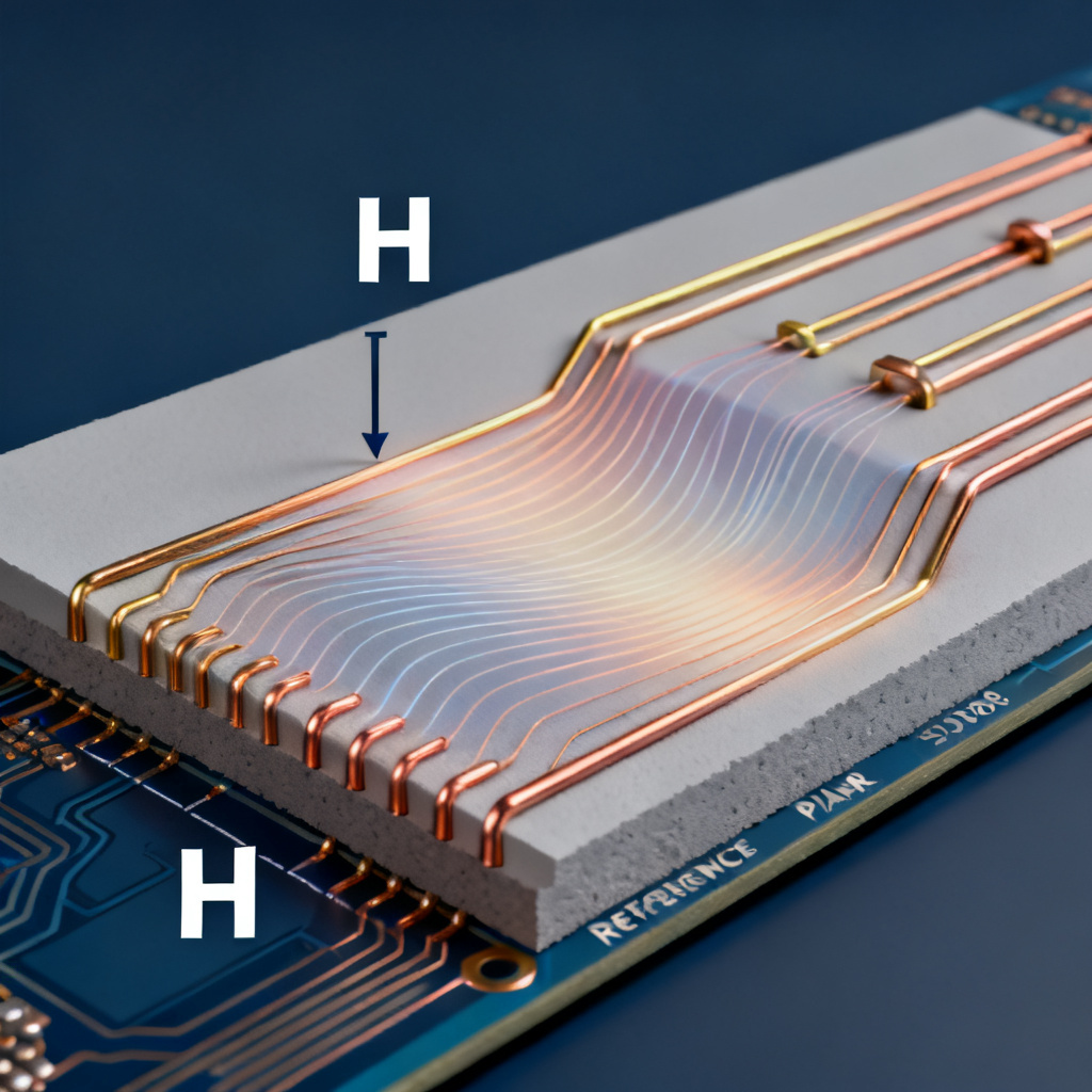
- Edge coupling: The field between the two traces (S).
- Broadside coupling: The field from each trace to the reference plane (H).
When H increases, the field lines to the reference plane become longer and weaker. This forces more of the field to couple between the two traces. As a result:
- The mutual inductance and capacitance increase.
- The differential impedance (Zdiff) decreases.
Conversely, when H decreases, the field to the plane is stronger, reducing trace-to-trace coupling and increasing Zdiff.
Key Formula Relationship
The fundamental equation shows how dielectric height (H) changes differential pair impedance:
[Z_diff ≈ (120/√ε_r) · ln(2H/(0.67W+0.8T)) · (1 – 0.48 · exp(-0.96 · S/H))]
Here, H appears in two critical places:
- The natural logarithm term – directly scales impedance.
- The exponential term – controls how much coupling exists between traces. As H increases, the exponential term becomes less negative, reducing the overall impedance.
Why Dielectric Height (H) is the Most Sensitive Variable for Impedance Control
Dielectric height (H) changes differential pair impedance with dramatically higher sensitivity than other parameters.
Impedance Change per Mil of H
For a typical 50 Ω single-ended trace or 100 Ω differential pair:
- ±1 mil change in H → ±2 to ±4 Ω change in Zdiff.
- ±1 mil change in trace width (W) → ±0.5 to ±1 Ω change.
- ±1 mil change in spacing (S) → ±0.2 to ±0.5 Ω change.
This means H is 4–8 times more sensitive than trace width, and 10–20 times more sensitive than spacing.
Why Fabrication Tolerance Matters
Standard PCB fabrication tolerances for dielectric height are typically ±10% of the target thickness. For a 4-mil prepreg layer, this means ±0.4 mil variation. That alone can cause a ±1.6 Ω impedance variation. Combined with other tolerances, it is easy to exceed the ±10% impedance tolerance commonly required for high-speed designs.
Real-World Example
A 100 Ω differential pair designed with H = 4 mil, W = 5 mil, S = 8 mil, T = 1.4 mil, Dk = 4.2. If the actual H becomes 4.5 mil (due to prepreg resin flow or core thickness variation), Zdiff drops to ~96 Ω—a 4% error. If H becomes 3.5 mil, Zdiff rises to ~104 Ω. This is often enough to cause signal integrity issues at 10+ Gbps.
Dielectric Height (H) and Differential Pair Impedance: Practical Implications
Understanding how dielectric height (H) changes differential pair impedance directly impacts design and fabrication decisions.
Stackup Design is Critical
The dielectric height between signal and reference plane is determined by the prepreg and core thicknesses in the stackup. Designers must:
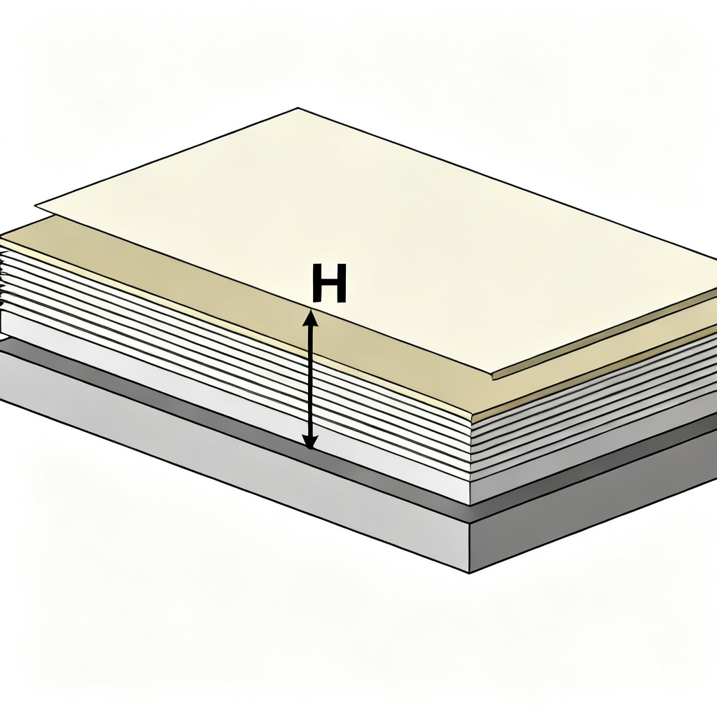
- Choose prepreg materials with tight thickness tolerances (e.g., 2116, 1080, 1067).
- Avoid using multiple layers of thin prepreg if a single thicker layer can achieve the same H—multiple layers increase variation.
- Specify controlled impedance requirements to the fabricator, including target H and tolerance.
The “H/S Ratio” Rule of Thumb
Per differential pair routing rules, a common design guideline is to keep the ratio H/S (dielectric height to trace spacing) between 1 and 3. When H/S < 1, the traces are too close to the plane, and differential impedance becomes dominated by the plane, making Zdiff very sensitive to H. When H/S > 3, the traces are too far from the plane, and impedance becomes dominated by trace-to-trace coupling, again making Zdiff highly sensitive to H. The sweet spot is H/S ≈ 1.5–2.5.
Fabrication Compensation
Fabricators can compensate for H variation by adjusting trace width (W) during etching, but this is limited:
- If H is too high, you can widen the traces to lower impedance—but only within the design rule limits.
- If H is too low, you can narrow the traces—but this may cause etching issues or violate minimum width rules.
The best approach is to design for the nominal H and specify a tight tolerance (±0.5 mil or better) on the dielectric thickness.
Case Studies: Dielectric Height (H) Changes Differential Pair Impedance in Real Designs
These case studies demonstrate exactly how dielectric height (H) changes differential pair impedance in practice.
Case Study 1: 100 Ω Differential Pair on FR4
| Dielectric Height H (mil) | Differential Pair Impedance Zdiff (Ω) | Impedance Variation (%) |
|---|---|---|
| 3.5 | 104.2 | +4.2% |
| 4.0 | 100.0 | 0% |
| 4.5 | 96.1 | -3.9% |
| 5.0 | 92.5 | -7.5% |
At H = 5.0 mil (a 25% increase), Zdiff drops below 95 Ω, exceeding the ±10% tolerance. This shows that even a small stackup error can push impedance out of spec.
Case Study 2: 90 Ω Differential Pair for USB 3.0
| Dielectric Height H (mil) | Differential Pair Impedance Zdiff (Ω) | Impedance Variation (%) |
|---|---|---|
| 5.5 | 93.5 | +3.9% |
| 6.0 | 90.0 | 0% |
| 6.5 | 86.8 | -3.6% |
| 7.0 | 83.9 | -6.8% |
Here, a 1-mil increase in H causes a 3.4% impedance drop. While still within ±15% tolerance, it leaves no room for other variables. If trace width also varies, the design may fail.
Best Practices for Managing Dielectric Height (H) Sensitivity in Differential Pair Impedance
Since dielectric height (H) changes differential pair impedance so dramatically, follow these best practices.
1. Use Thicker Dielectrics When Possible
Thicker dielectrics reduce the percentage variation in H. For example, a 0.5-mil variation on a 4-mil layer is 12.5%, but on an 8-mil layer it is only 6.25%. However, thicker dielectrics also increase trace width requirements for a given impedance, which may conflict with routing density.
2. Specify Controlled Impedance with H Tolerance
When sending a stackup to the fabricator, include:
- Target impedance (e.g., 100 Ω ±10%)
- Target dielectric height (e.g., 4.0 mil ±0.5 mil)
- Material type (e.g., FR4 with Dk = 4.2 ±0.1)
3. Use Impedance Coupons
Include test coupons on the panel that replicate the exact stackup and trace geometry. After fabrication, measure Zdiff and compare to the target. If H variation is suspected, request cross-sectioning to verify actual dielectric thickness.
4. Simulate Worst-Case Tolerances
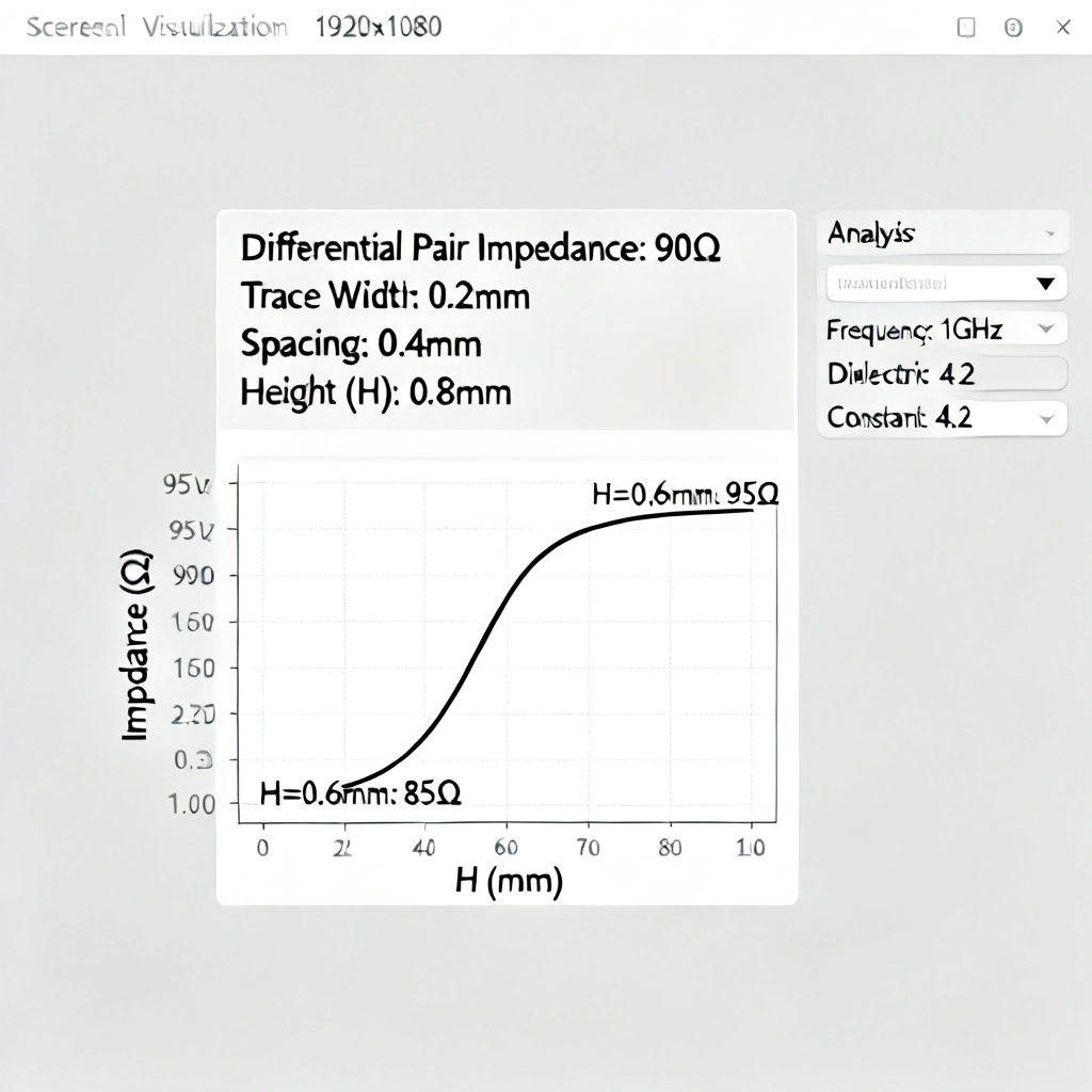
Use tools like Polar Si9000, HyperLynx, or Ansys Q2D Extractor to simulate the full range of H variation (min, nom, max). Ensure that even at the extremes, Zdiff stays within your required tolerance.
5. Avoid Thin Prepregs for High-Speed Signals
Thin prepregs (e.g., 1067 at ~2 mil) are highly sensitive to resin flow and copper roughness. For high-speed differential pairs, prefer thicker prepregs (2116, 1652, or 7628) to reduce H variation.
Why Choose Our Custom High-Speed PCB Manufacturing

We specialize in tight-tolerance dielectric height control for reliable 100 Ω and 90 Ω differential pairs. Unlike generic fabricators, we:
- Use advanced prepreg selection and lamination processes to maintain H within ±0.3 mil.
- Provide free impedance simulation and stackup recommendations for your design.
- Include impedance coupons with every panel for verified performance.
Our approach ensures that dielectric height (H) changes differential pair impedance within your required tolerance, not beyond it.
Frequently Asked Questions About Dielectric Height (H) and Differential Pair Impedance
How does dielectric height (H) change differential pair impedance?
Dielectric height (H) changes differential pair impedance by altering the electromagnetic field distribution. Increasing H reduces impedance by forcing more field coupling between traces, while decreasing H increases impedance by strengthening the field to the reference plane.
Why is dielectric height (H) the most sensitive variable for impedance control?
Dielectric height (H) changes differential pair impedance with 4-8 times more sensitivity than trace width and 10-20 times more than spacing. A ±1 mil change in H can cause ±2 to ±4 Ω impedance shift, making it the dominant variable in high-speed PCB design.
What is the ideal H/S ratio for differential pair impedance control?
The ideal H/S ratio (dielectric height to trace spacing) is between 1.5 and 2.5. This range minimizes the sensitivity of how dielectric height (H) changes differential pair impedance while maintaining good signal integrity.
How can I compensate for dielectric height variation in fabrication?
Since dielectric height (H) changes differential pair impedance significantly, specify tight H tolerance (±0.5 mil), use impedance coupons, and simulate worst-case tolerances. We offer free stackup analysis to help you manage H variation.
Industry Terminology: Dielectric Height and Differential Pair Impedance
Dielectric height (H): The vertical distance between the signal layer and the reference plane, typically measured in mils or microns. This dimension directly controls how dielectric height (H) changes differential pair impedance.
Differential pair impedance (Zdiff): The impedance between two coupled traces carrying complementary signals, commonly 100 Ω or 90 Ω for high-speed interfaces.
Prepreg: A sheet of fiberglass pre-impregnated with resin, used to build up the dielectric layers in a PCB stackup. Its thickness variation is the primary cause of H tolerance issues.
Impedance coupon: A test structure on the PCB panel that replicates the production stackup and trace geometry for impedance verification.
Need Help with Your High-Speed PCB Stackup?
Contact our engineering team for a free impedance simulation and stackup recommendation. We specialize in tight-tolerance dielectric height control for reliable 100 Ω and 90 Ω differential pairs, ensuring that dielectric height (H) changes differential pair impedance within your design specifications.