[rank_math_breadcrumb]
In high-speed PCB design, understanding differential pair impedance trade-offs between tight and loose coupling is critical for signal integrity. This guide explains the key differences, impedance control strategies, and practical design choices for B2B engineers and procurement specialists.
Introduction: The Foundation of High-Speed PCB Design
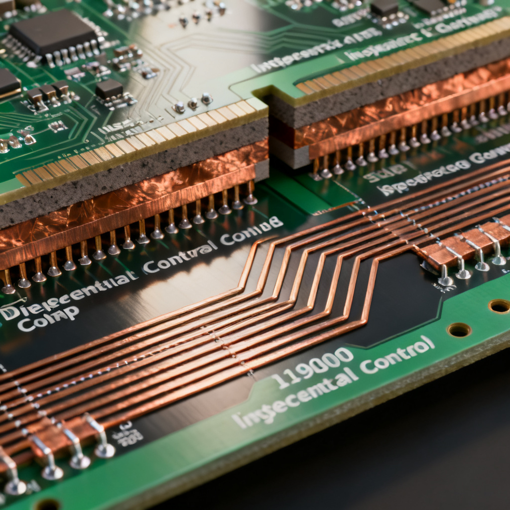
In high-speed PCB design, differential pairs are the backbone of reliable signal transmission. Whether designing for Gigabit Ethernet, USB 3.0, HDMI, or PCIe, understanding differential pair impedance trade-offs between tight and loose coupling is essential. This pillar content synthesizes industry-leading insights to provide a comprehensive guide for B2B PCB engineers and procurement specialists, covering definitions, impedance control, and real-world trade-offs.
What Are Differential Pairs and Why Does Coupling Matter?
A differential pair consists of two transmission lines carrying equal and opposite signals, with signal integrity determined by differential pair impedance (Zdiff). The coupling between these traces—how close they are to each other—directly influences impedance, crosstalk, and manufacturability. Tight coupling refers to traces placed very close together (small edge-to-edge spacing), while loose coupling involves wider spacing. The choice between these approaches is a trade-off affecting signal performance, PCB stack-up design, and cost.
Key Definitions from Industry Experts
Differential Impedance (Zdiff): The impedance seen by a differential signal, calculated as Zdiff = 2 × Z0 × (1 – k), where Z0 is the single-ended impedance and k is the coupling coefficient. Tight coupling increases k, reducing Zdiff for a given trace width.
Coupling Coefficient (k): A measure of electromagnetic interaction between traces. Tight coupling yields k > 0.3, while loose coupling has k < 0.1.
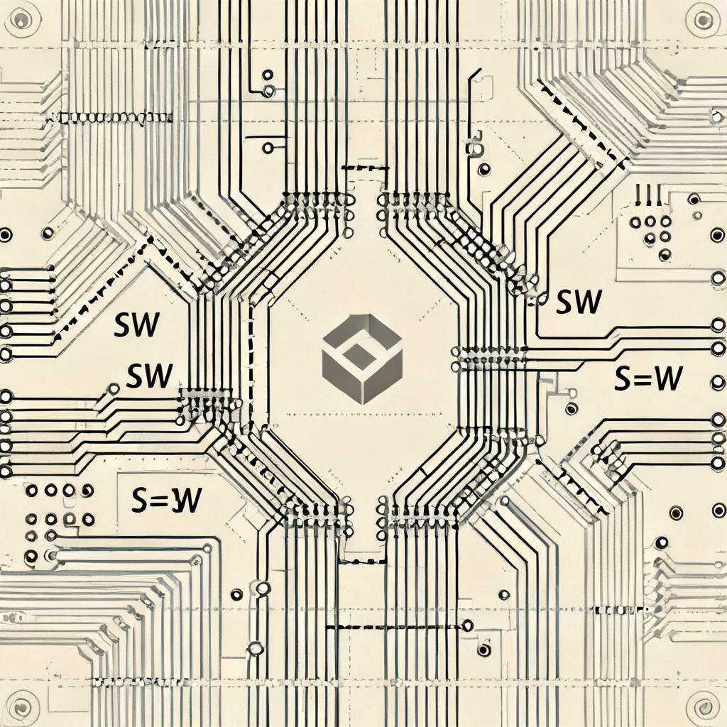
Tight Coupling: Typically achieved with spacing (S) less than or equal to the trace width (W), often S ≤ W. This enhances common-mode rejection but complicates impedance control.
Loose Coupling: Achieved with S > 2W or even S > 3W. This simplifies design but may increase crosstalk and require wider traces.

The Trade-Offs: A Deep Dive into Tight vs. Loose Coupling
1. Impedance Control and Signal Integrity
Differential pair impedance control is the primary trade-off. Tight coupling offers better common-mode noise rejection because the fields are more confined between the traces, reducing external electromagnetic interference (EMI). However, it makes impedance highly sensitive to manufacturing tolerances. A small variation in spacing (e.g., ±10% due to etching) can cause a significant impedance shift, potentially exceeding ±15% of the target Zdiff. This is critical for high-speed standards like PCIe Gen 4/5, where tight impedance tolerance (±5%) is mandatory.
Loose coupling provides more stable impedance control because the traces are less influenced by each other. The single-ended impedance (Z0) dominates, and Zdiff is approximately 2 × Z0. This reduces sensitivity to spacing variations, making it easier to achieve tight impedance tolerances (e.g., ±5%) in mass production. However, loose coupling increases the loop area, which can lead to higher radiated EMI and susceptibility to external noise.
The trade-off is a balance: tight coupling minimizes differential-to-common-mode conversion (important for high-speed serial links), but loose coupling simplifies stack-up design. In practice, for frequencies above 1 GHz, tight coupling is often preferred for its EMI benefits, but only if the PCB manufacturer can maintain precise etch tolerances.
Key Takeaway:
Tight Coupling: Better for EMI suppression and common-mode rejection; risk of impedance variation due to manufacturing tolerances.
Loose Coupling: Better for impedance stability and manufacturability; risk of higher EMI and noise susceptibility.
2. Crosstalk and Interference
In tightly coupled pairs, the near-end crosstalk (NEXT) between the two traces is inherently low because the signals are complementary and cancel each other out. However, far-end crosstalk (FEXT) can be significant if the traces are not perfectly symmetric. Tight coupling also reduces crosstalk to adjacent pairs due to field confinement.
Loose coupling increases the distance between traces, which reduces the mutual capacitance and inductance between them. This lowers NEXT and FEXT within the pair itself, but the traces become more susceptible to crosstalk from other signals on the board because the fields extend further into the dielectric. For dense PCB layouts, loose coupling may require additional shielding or ground planes.
The relationship between coupling and crosstalk is non-linear. For spacing greater than 2W, crosstalk drops exponentially, but the differential pair’s immunity to common-mode noise decreases. In mixed-signal designs, tight coupling is often used to isolate high-speed digital signals from analog sections.
Key Takeaway:
Tight Coupling: Low intra-pair crosstalk but sensitive to asymmetry; good for dense routing.
Loose Coupling: Low intra-pair crosstalk at wide spacing; but higher susceptibility to inter-pair crosstalk and external noise.
3. PCB Stack-Up and Impedance Target
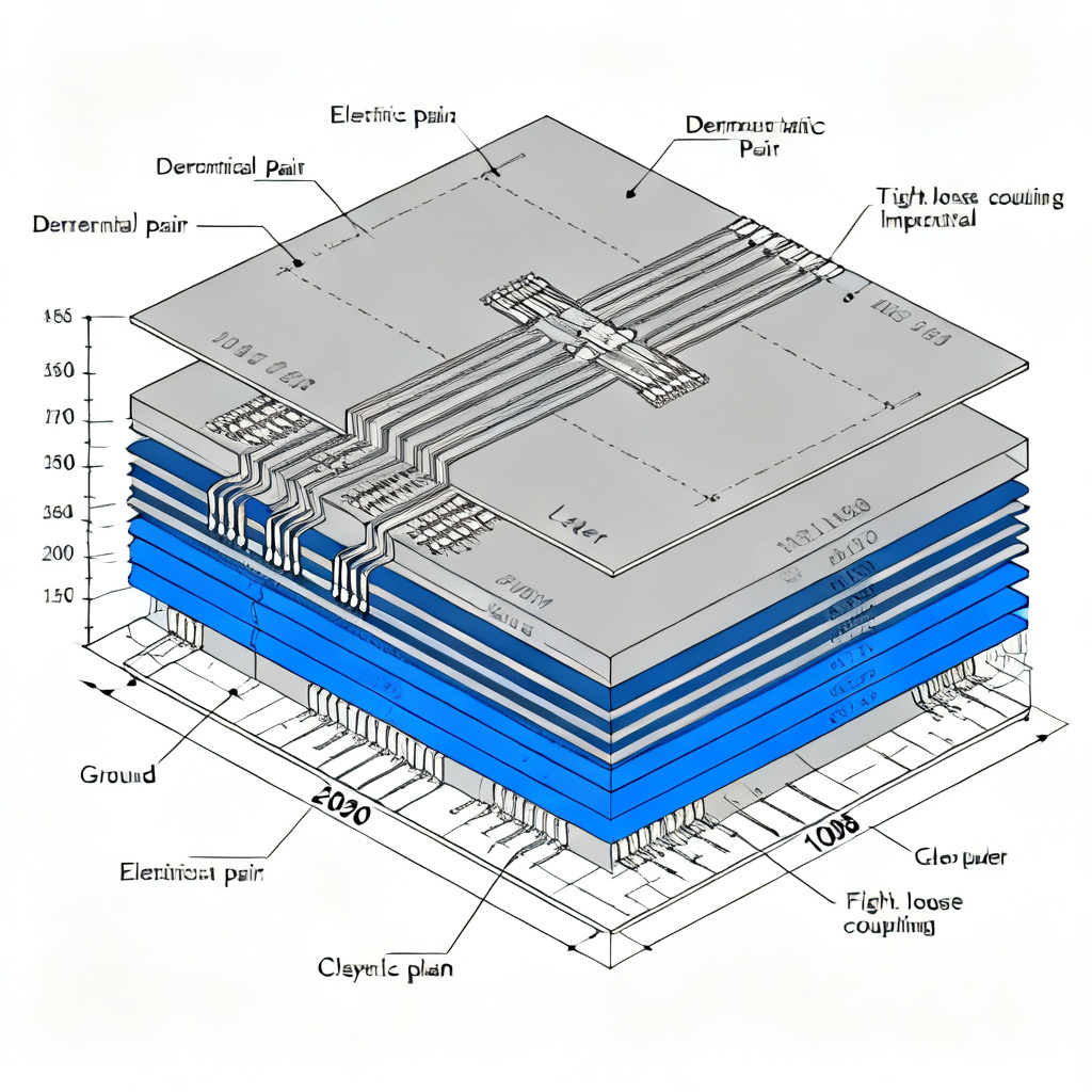
Tight coupling requires a specific stack-up design. The traces must be placed on a layer with a controlled dielectric (e.g., FR4 with low Dk variation). The reference plane (ground) must be close to the signal layer to maintain a low Z0. For tight coupling, the target Zdiff is often achieved by adjusting the trace width (W) and spacing (S). A common rule: for Zdiff = 100Ω, tight coupling might use W = 5 mil, S = 5 mil, with a dielectric thickness of 4 mil.
Loose coupling allows more flexibility in stack-up. The traces can be wider (e.g., W = 7 mil, S = 15 mil) to achieve the same Zdiff, reducing conductor losses. However, wider traces increase the board’s real estate usage, which can be problematic for high-density interconnect (HDI) designs. Loose coupling also requires a thicker dielectric to maintain Z0, which may increase the overall board thickness.
The choice of coupling affects the characteristic impedance of each trace. In tight coupling, the odd-mode impedance (Zodd) is lower than Z0, while in loose coupling, Zodd is close to Z0. This impacts termination and matching. For standard interfaces like USB 2.0 (Zdiff = 90Ω), loose coupling is common; for HDMI (Zdiff = 100Ω), tight coupling is typical due to the need for low EMI.
Key Takeaway:
Tight Coupling: Requires precise stack-up (thin dielectric, narrow traces); suitable for high-density boards.
Loose Coupling: More forgiving stack-up (wider traces, thicker dielectric); but consumes more board area.
4. Manufacturing and Cost Considerations
Tight coupling increases manufacturing complexity. The narrow spacing (e.g., 4 mil or less) requires advanced etching processes, which can lead to yield loss if not controlled. Additionally, tight coupling often necessitates tighter tolerance on dielectric thickness, driving up PCB fabrication costs. For high-volume production, this can be a significant factor.
Loose coupling is generally easier to manufacture. Wider spacing reduces the risk of etching defects and allows for lower-cost standard processes. However, if the traces become too wide, the PCB may require additional layers to accommodate routing, offsetting cost savings. Loose coupling also simplifies impedance testing because the differential impedance is less sensitive to variations.
The trade-off is clear: tight coupling offers better electrical performance but at a higher cost and lower yield. Loose coupling is more cost-effective for prototypes and medium-volume runs, but may not meet the stringent requirements of high-speed standards above 10 Gbps. For example, in PCIe Gen 5 (32 Gbps), tight coupling is almost mandatory to maintain signal integrity.
Key Takeaway:
Tight Coupling: Higher cost due to tighter tolerances; better for high-speed, low-EMI applications.
Loose Coupling: Lower cost and higher yield; suitable for moderate-speed designs.
5. Real-World Application Examples
In high-speed serial links like SATA (6 Gbps) and USB 3.0 (5 Gbps), tight coupling is preferred because the signals are differential and require low EMI. The typical design uses S = W (e.g., 5 mil spacing) with a ground plane 4 mil below. This ensures Zdiff = 100Ω and common-mode rejection.
For lower-speed interfaces like I2C or SPI (differential variants), loose coupling is acceptable. In these cases, the priority is cost and manufacturability. A common example is a differential pair for a 100 MHz clock: S = 3W is used to simplify the stack-up.
In RF and microwave designs (e.g., 5G antennas), tight coupling is essential for impedance matching and to minimize radiation. However, for power delivery networks (PDNs), loose coupling is used to avoid excessive capacitance between traces.
Differential Pair Impedance Parameters Table
| Parameter | Tight Coupling (S ≤ W) | Loose Coupling (S ≥ 3W) |
|---|---|---|
| Spacing (S) | ≤ Trace Width (W) | ≥ 3 × Trace Width (W) |
| Coupling Coefficient (k) | > 0.3 | < 0.1 |
| Impedance Sensitivity | High (sensitive to etch tolerances) | Low (stable with manufacturing variations) |
| EMI Performance | Excellent (confined fields) | Moderate (larger loop area) |
| Common-Mode Rejection | High | Low |
| Manufacturing Cost | Higher (tight tolerances) | Lower (standard processes) |
| Typical Applications | PCIe Gen 5, HDMI, USB 3.0 | I2C, SPI, 100 MHz clocks |
Industry Terminology Explained
Differential Impedance (Zdiff): The impedance a differential signal sees, calculated from trace geometry and dielectric properties. It is the primary metric for high-speed differential pairs.
Coupling Coefficient (k): A dimensionless parameter quantifying electromagnetic interaction between two traces. High k indicates tight coupling.
Odd-Mode Impedance (Zodd): The impedance of one trace in a differential pair when driven by a differential signal. It is lower than the single-ended impedance Z0 in tight coupling.
Common-Mode Rejection: The ability of a differential pair to suppress noise that appears identically on both traces. Tight coupling enhances this property.
Far-End Crosstalk (FEXT): Noise induced at the far end of a victim trace due to signals on an aggressor trace. Tight coupling can reduce FEXT within the pair.
Practical Design Guidelines for High-Speed PCBs
Based on the integrated insights, here are actionable guidelines for your B2B PCB projects:
- Determine the Target Impedance and Standard: For common high-speed standards (e.g., PCIe, HDMI, USB 3.0), aim for Zdiff = 100Ω or 90Ω. Refer to the specific standard’s requirements (e.g., PCIe Gen 5 requires ±5% tolerance). Use a field solver (e.g., Polar Si9000, Ansys Q3D) to calculate W and S based on your stack-up.
- Choose Coupling Based on Speed and Layout Density: Tight coupling (S ≤ W) for frequencies > 1 GHz, high-density boards, or when EMI is a concern (e.g., S = 0.8W for HDMI). Loose coupling (S ≥ 3W) for frequencies < 500 MHz, prototypes, or when manufacturing cost is critical (e.g., S = 4W for a 100 MHz clock).
- Optimize the Stack-Up: For tight coupling, use a thin prepreg (e.g., 1080 or 2116) to keep dielectric thickness low (e.g., 4 mil). Ensure the reference plane is continuous (no split planes under the pair). For loose coupling, use a thicker core (e.g., 8 mil) to maintain Z0. Avoid placing the pair near board edges to prevent impedance discontinuities.
- Account for Manufacturing Tolerances: For tight coupling, specify ±10% on spacing and ±5% on trace width in fabrication notes. Request impedance test coupons for verification. For loose coupling, standard tolerances (±20% on spacing) are usually sufficient. Use a 10% tolerance on Zdiff for cost savings.
- Simulate and Validate: Use 3D electromagnetic simulation (e.g., HFSS, CST) for critical high-speed pairs. For tight coupling, simulate the effect of glass weave (fiber weave effect) on impedance variation. For loose coupling, focus on crosstalk to adjacent traces. Add ground vias (stitching vias) if needed.
Conclusion: Making the Right Choice for Your B2B PCB Order
The trade-off between tight and loose coupling in differential pair impedance is not a one-size-fits-all decision. For high-speed, high-reliability applications (e.g., 5G, data centers, automotive ADAS), tight coupling is the gold standard, offering superior signal integrity and EMI performance at the cost of manufacturing complexity. For cost-sensitive or moderate-speed designs (e.g., industrial control, consumer IoT), loose coupling provides a robust, manufacturable solution.
As a B2B PCB supplier specializing in high-speed boards, we recommend the following approach:
- Prototype Phase: Use loose coupling to reduce risk and cost, then refine to tight coupling for production if needed.
- Production Phase: For high-volume orders, invest in tight coupling with tight tolerance control to ensure first-pass yield and meet customer specifications.
By understanding these trade-offs, you can design differential pairs that meet both electrical and manufacturing requirements, ensuring your high-speed PCB projects succeed. For custom impedance control and stack-up design support, contact our engineering team today.
Frequently Asked Questions
What is the main difference between tight and loose coupling for differential pair impedance?
The main difference lies in the spacing between traces: tight coupling uses spacing ≤ trace width, enhancing common-mode rejection and EMI performance but increasing manufacturing sensitivity. Loose coupling uses wider spacing (≥3W), simplifying impedance control and reducing cost but potentially increasing crosstalk and noise susceptibility.
How does differential pair impedance affect high-speed PCB signal integrity?
Differential pair impedance directly impacts signal integrity by determining reflection, attenuation, and crosstalk. Mismatched impedance causes signal degradation, while controlled impedance (e.g., 100Ω for HDMI) ensures clean transmission. Tight coupling improves common-mode rejection, while loose coupling offers more stable impedance control.
When should I use tight coupling for differential pairs in my PCB design?
Use tight coupling for high-speed interfaces above 1 GHz (e.g., PCIe Gen 5, HDMI, USB 3.0) where EMI suppression and common-mode rejection are critical. It is also ideal for dense PCB layouts where space is limited, but requires precise manufacturing tolerances.
What are the cost implications of tight vs loose coupling for differential pair impedance?
Tight coupling increases PCB fabrication costs due to tighter tolerances on spacing and dielectric thickness, potentially reducing yield. Loose coupling is more cost-effective for prototypes and moderate-speed designs, as it uses standard processes and wider tolerances.
Can I use loose coupling for high-speed differential pairs above 10 Gbps?
Generally, loose coupling is not recommended for data rates above 10 Gbps (e.g., PCIe Gen 5 at 32 Gbps) because it increases EMI and reduces common-mode rejection. Tight coupling is almost mandatory to meet signal integrity requirements at these speeds.