In high-speed PCB design, reference plane continuity is the most critical rule for ensuring a proper return path. Without it, signal integrity fails, EMI spikes, and your board may not function reliably above 100 MHz. This page explains the physics, consequences, and practical solutions to master return path design.
The Physics of Return Current – Why It Follows the Signal
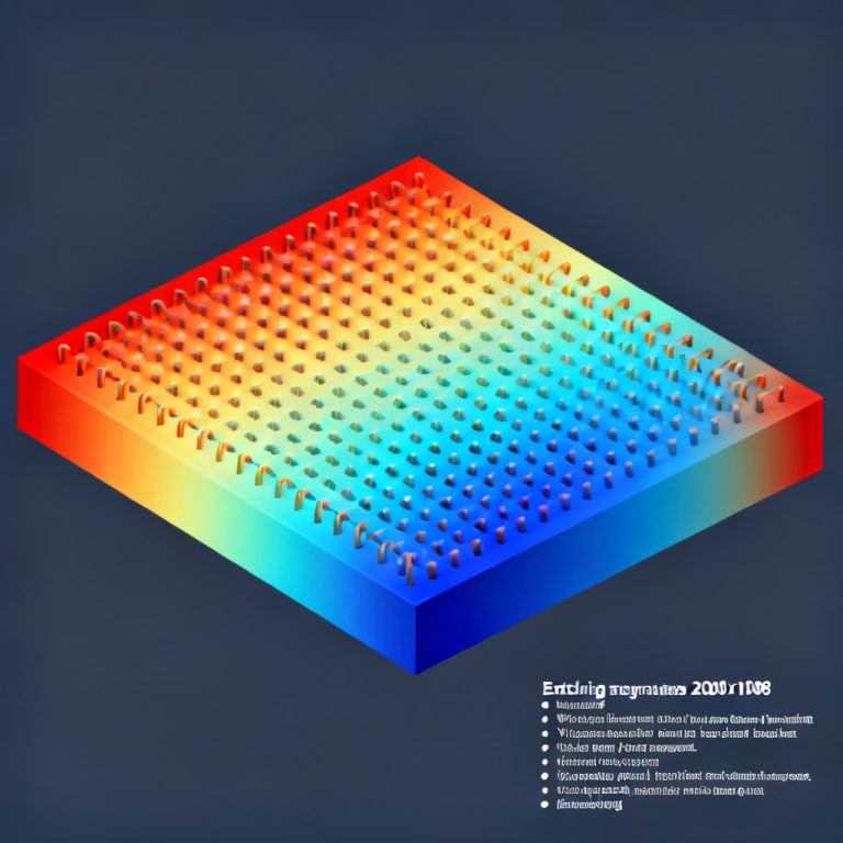
To master reference plane continuity, you must first understand return current behavior at high frequencies. At DC, current follows the path of least resistance. But above 100 MHz, inductive reactance dominates, and return current follows the path of least inductance—directly beneath the signal trace on the adjacent reference plane.
Principle of Least Inductance
At high frequencies, return current minimizes loop area. It flows in a narrow band on the reference plane, directly under the trace. This is called the image plane effect.
Return Current Density
In microstrip, return current concentrates within 3-4 times the trace width. In stripline, it splits between the two reference planes, with most on the closer plane.
Consequences of a Broken Return Path
When a signal crosses a discontinuity in its reference plane continuity, multiple problems occur simultaneously.
Increased Loop Inductance
The forced detour creates a larger current loop, increasing inductance and causing impedance spikes, reflections, and signal degradation.
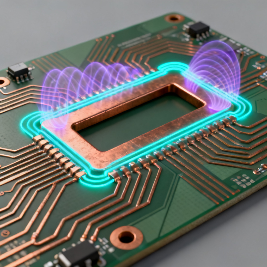
Common-Mode Radiation (EMI)
A slot or split in the reference plane acts as an antenna. The detoured return current radiates at harmonic frequencies, often causing FCC/CE failure.
Crosstalk and Ground Bounce
Shared detour paths create shared inductance, leading to simultaneous switching noise (SSN) and crosstalk between signals.
Signal Integrity Failures
Protocols like DDR, PCIe, USB 3.0 suffer eye closure, jitter, and bit errors when return path is broken.
How to Design for Continuous Return Paths
Here are actionable techniques to ensure reference plane continuity in your high-speed PCB design.
The Golden Rule
Never route a high-speed signal across a split plane. This includes gaps between analog/digital ground, slots for connectors, or changes from ground to power reference.
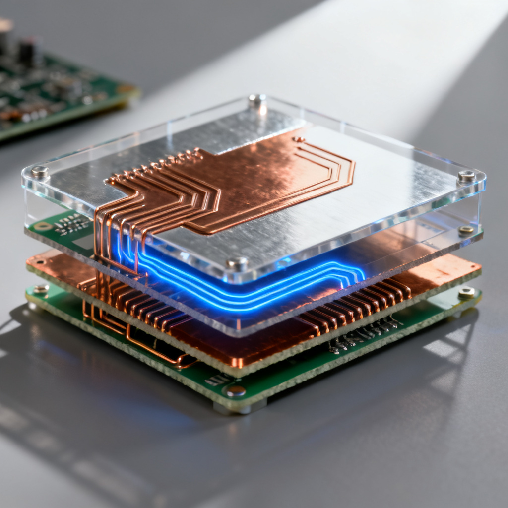
Proper Layer Stack-Up
For a 4-layer board: Layer 1 (signal), Layer 2 (solid GND), Layer 3 (power), Layer 4 (signal). High-speed signals on Layer 1 reference the continuous GND plane. For 6+ layers, alternate signal and reference planes.
Via Stitching
When a signal changes layers, place a stitching via (ground via) within 30-50 mils of the signal via. This provides a low-inductance path for return current. For differential pairs, use a stitching via pair.
Avoiding Slots and Cutouts
Never route high-speed traces across slots. Use copper bridges across unavoidable slots and route signals over the bridges. For isolation gaps, use a single solid ground plane with physical separation.
Power Plane as Reference
If using a power plane as reference, ensure it is continuous and well-decoupled to ground via capacitors placed near ICs.
Practical Layout Rules and Guidelines
Apply these rules to maintain reference plane continuity in every design.
| Rule | Description |
|---|---|
| 3W Rule for Return Path | Keep solid ground under trace for 3x trace width on each side. |
| Via Stitching Density | One stitching via per signal via for layer changes. For slots, stitch every 1/10 wavelength. |
| Avoid Long Return Path Loops | Minimize loop area = trace length × distance to reference plane. |
| Decoupling Capacitors | Place near ICs to provide AC return path from power to ground. |
| Differential Pairs | Keep reference plane continuous. Use stitching via pairs for layer transitions. |
| Guard Traces and Ground Fills | Use guard traces for sensitive signals. Stitch ground fills to main plane. |
Advanced Considerations
These advanced topics require careful reference plane continuity planning.
Mixed-Signal Designs
Use a single solid ground plane. Separate analog and digital components physically. If a moat is needed, provide a copper bridge for signals.
High-Density Interconnect (HDI)
Use staggered microvias to avoid voids. Each signal via needs a ground via within 0.5 mm.
High-Speed Protocols
DDR: Ensure VDDQ plane is continuous and decoupled. PCIe: Use solid ground reference. USB 3.2: Connect shield to ground with multiple vias.
Common Mistakes and How to Fix Them
| Mistake | Consequence | Fix |
|---|---|---|
| Routing over split ground | High EMI, reflections | Re-route or add bridge |
| Layer change without stitching via | Large loop inductance | Add ground via within 50 mils |
| Power plane reference without decoupling | Poor return path | Add decoupling caps near ICs |
| Floating copper island | Antenna radiation | Stitch to ground every 1/8 wavelength |
| Differential pair across slot | Common-mode noise | Re-route or add ground bridge |
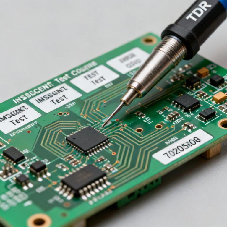
At [Your Company Name], we manufacture high-speed PCBs with controlled impedance, multi-layer stack-ups up to 40 layers, HDI technology, and rigorous TDR testing. Our expertise ensures your design meets the most critical rule of return path design. Contact us for a free design review.
Frequently Asked Questions
What is reference plane continuity in PCB design?
Reference plane continuity means the return current path for a high-speed signal is uninterrupted, typically provided by a solid ground or power plane directly adjacent to the signal trace.
Why is return path important for signal integrity?
A continuous return path minimizes loop inductance, prevents EMI, and maintains consistent impedance, which is essential for high-speed signal integrity.
How do you fix a broken return path?
Use via stitching for layer transitions, avoid routing over slots, add copper bridges across unavoidable gaps, and ensure solid reference planes in the stack-up.
Can a power plane be used as a reference plane?
Yes, if the power plane is continuous and has low AC impedance to ground via decoupling capacitors placed near the ICs.
What are common return path mistakes?
Routing across split planes, missing stitching vias, unstitched ground fills, and using power planes without decoupling are common mistakes.