Impedance control is the core technical requirement for high-speed digital, RF, 5G, automotive, medical and aerospace PCBs. It ensures signal integrity by stabilizing characteristic impedance within a defined tolerance, avoiding signal reflection, crosstalk and timing errors. This all-in-one pillar guide explains what impedance control pcb manufacturing means, key manufacturing variables, standard production workflow, impedance coupon design rules, tolerance classification & cost, TDR testing principles, and a practical checklist. Aligned with IPC industry standards and real PCB factory mass production experience, it helps design engineers, procurement buyers and hardware project managers correctly specify, verify and audit controlled impedance PCBs while balancing performance, process capability and budget.
The PCB Manufacturing & Testing Guidelines, which covers all manufacturing processes from prototype to mass production, provides essential context for understanding impedance control. This guide focuses specifically on impedance control within that framework.
Table of Contents
- 1. What Is Impedance Control in PCB Manufacturing
- 2. Why Controlled Impedance Matters for High-Speed & RF Applications
- 3. Key Production Variables Affecting PCB Impedance
- 4. Standard Impedance Control Process Flow From Design to Mass Production
- 5. Impedance Coupon Design Rules for Valid Real Test Data
- 6. PCB Impedance Tolerance Grades, Process Capability & Cost Premium
- 7. TDR Testing Principle, Sampling Standard and Report Requirement
- 8. Complete Impedance Control Checklist for Designers & Buyers
- 9. Key Takeaways
- 10. FAQ About PCB Impedance Control
- 11. Get Professional Impedance Control Stackup & Quotation Support
What Is Impedance Control in PCB Manufacturing
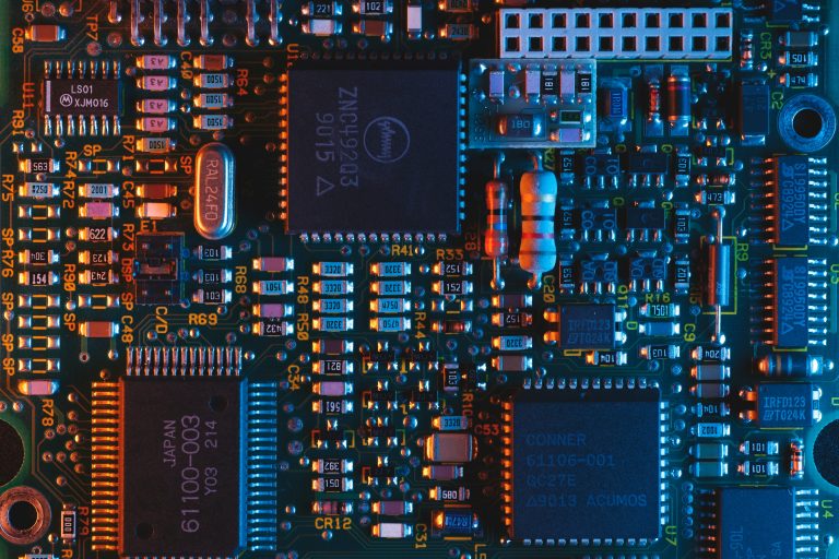
Impedance control pcb manufacturing is the precise fabrication capability to deliver printed circuit boards that strictly match the target characteristic impedance defined in high-speed design stackup. Unlike regular PCB production that only guarantees electrical connectivity and layer alignment, impedance-controlled manufacturing must lock physical structure, material properties and process stability together to maintain consistent electrical performance across batches.
The biggest difficulty comes from multi-variable coupling: trace width after etching, dielectric thickness, material Dk (dielectric constant), copper foil weight and solder mask thickness all interact to cause impedance drift. No single parameter can be adjusted independently.
The core goals of professional impedance control are:
- Maintain actual impedance within specified tolerance
- Ensure batch-to-batch consistency for mass production
- Comply with IPC international manufacturing standards
- Eliminate signal integrity risks caused by impedance discontinuity
Design-side impedance calculations are covered in Impedance Matching Ultimate, which complements the manufacturing focus of this guide. Impedance control is never only a design task or a pure factory task — it is a joint result of high-speed design calculation, material selection, standardized fabrication process, and strict quality testing.
Why Controlled Impedance Matters for High-Speed & RF Applications
Modern electronic products rely more on high-speed transmission interfaces such as PCIe, USB4, HDMI, Ethernet, 5G RF and automotive CAN/LIN. Without accurate impedance control pcb manufacturing, common failures include:
- Signal reflection and waveform distortion
- Severe crosstalk between adjacent traces
- Timing delay mismatch and system unstable reboot
- RF signal attenuation and poor communication distance
- Low yield and high rework cost in mass production
For global industrial buyers and engineers, clear impedance specification and factory process capability verification become essential supplier audit items, especially for medical, aerospace, automotive and industrial control projects that require long-term reliability.
Layer arrangements for controlled impedance are detailed in Stackup Design, providing essential background for understanding how stackup choices affect manufacturability.
Key Production Variables Affecting PCB Impedance
Each manufacturing parameter has its own natural fluctuation range and different impact on final impedance. The following table summarizes the most critical factors, fluctuation scope and influence level (referenced from IPC standard and top PCB manufacturer mass production data):
| Production Variable | Typical Fluctuation Range | Impedance Impact |
|---|---|---|
| Etching Trace Width | ±0.5–1.0 mil | High |
| Dielectric Thickness | ±5–10% | High |
| Material Dk Batch Variation | ±2–5% | Medium |
| Copper Foil Thickness | ±0.1–0.3 oz | Low to Medium |
| Solder Mask Thickness | 0.5–1.0 mil | Low |
Core explanation: Etching width and dielectric thickness are the two dominant factors, responsible for most impedance deviation. Over-etching narrows traces and raises impedance; under-etching widens traces and lowers impedance.
Dk variation from different material batches brings gradual impedance drift across production lots. Material properties that affect Dk are analyzed in PCB Materials Selection. Copper thickness affects conductor cross-section and skin effect, while solder mask only creates minor interference for standard microstrip and stripline structures.
Optimizing these two high-impact variables first can greatly improve impedance stability and production yield in impedance control pcb manufacturing.
Standard Impedance Control Process Flow From Design to Mass Production
Professional PCB factories follow a closed-loop standardized workflow to guarantee impedance performance:
Step 1: Stackup Definition & Impedance Calculation
Designers confirm layer structure, select core/prepreg material Dk value, and calculate theoretical trace width for target impedance.
Step 2: First Article Impedance Coupon Test
Before mass production, fabricate the first panel and test impedance coupons to collect actual deviation data.
Step 3: Etching Line Width Compensation & Process Tuning
Engineers adjust etching parameters to offset inherent process deviation, making actual impedance close to design target.
Step 4: Mass Production with SPC Statistical Process Control
Monitor key parameters in real time: line width, lamination thickness, pressure and material batch consistency to avoid process drift.
Step 5: Final TDR Sampling Inspection & Shipment
Finished boards are sampled by TDR testing; only batches within tolerance are released for delivery.
This full flow turns theoretical design into stable mass production output, which is the key benchmark for global buyers to evaluate a PCB supplier’s capability.
Impedance Coupon Design Rules for Valid Real Test Data
Impedance coupons are the standard test vehicle to reflect real board impedance performance. Improper coupon design leads to invalid TDR data and hidden quality risks. Follow these universal rules for impedance control pcb manufacturing:
- Representativeness: The coupon must use the same layer, stackup, copper weight and dielectric material as the actual functional traces; simplified structure is not allowed.
- Placement: Arrange coupons on process edge or board edge copper-free area, avoiding panel warpage and high-density routing zones.
- Minimum Length: Coupon length ≥ 6 inches to ensure TDR captures stable and interference-free readings.
- Clear Marking: Label target impedance value, layer number, copper thickness and stackup version for full batch traceability.
Well-designed coupons ensure TDR test data is credible and can guide process calibration effectively.
PCB Impedance Tolerance Grades, Process Capability & Cost Premium
Impedance tolerance directly decides factory process requirements, production difficulty and unit cost. Three industry mainstream grades are widely adopted in impedance control pcb manufacturing:
| Tolerance Grade | Allowed Tolerance | Process Capability Requirement | Cost Premium |
|---|---|---|---|
| Standard | ±10% | Standard production line with basic process monitoring | Baseline |
| Strict | ±7% | Enhanced SPC, frequent machine calibration, strict material batch screening | +10% ~ 20% |
| Precision | ±5% | Dedicated production line, fixed stable Dk material, full inline inspection | +25% ~ 40% |
±10% offers the best cost-performance for consumer electronics and general high-speed digital products. ±7% suits automotive, industrial control and mid-range RF applications requiring higher stability. ±5% should only be used for aerospace, medical and high-frequency premium RF projects — over-specifying will cause unnecessary cost increase.
Engineers and buyers should select tolerance grade reasonably based on application scenario instead of blindly pursuing ultra-precision.
TDR Testing Principle, Sampling Standard and Report Requirement
TDR (Time Domain Reflectometry) is the universal industry test method for PCB controlled impedance, compliant with IPC-TM-650 standard.
How TDR Works
TDR launches a fast rise-time pulse into the impedance coupon. When the pulse meets impedance discontinuity caused by trace width, thickness or material change, signal reflection occurs. The instrument analyzes reflection time and amplitude, then generates an impedance-distance curve showing impedance fluctuation along the trace.
Industry Sampling Standard
– Per production batch, every unique target impedance value must test 5–10 coupons at least
– Test report must include average impedance, min/max value and complete waveform curve
– Official TDR reports should be provided together with shipment documents for customer audit
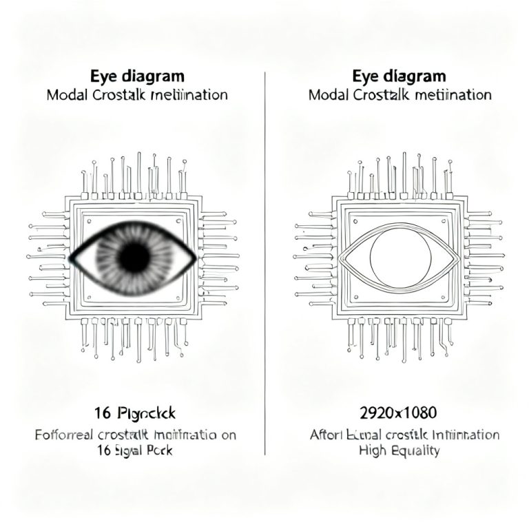
TDR testing is the final quality gate to confirm whether the batch meets impedance specifications. Signal quality testing that complements TDR measurements is covered in Eye Diagram and Jitter Analysis, helping verify that impedance control translates to good signal integrity.
Complete Impedance Control Checklist for Designers & Buyers
Use this checklist to avoid omission in design handoff, DFM review and supplier confirmation for impedance control pcb manufacturing:
- Clearly define all target impedance values and corresponding tolerance grade (±10% / ±7% / ±5%)
- Provide complete official stackup file with trace width, copper weight and dielectric parameters
- Design impedance coupons strictly following standard layout rules and verify structure consistency
- Confirm the PCB factory’s actual process capability matches your required tolerance level
- Require the supplier to provide official TDR test reports for every production batch
Key Takeaways
- Impedance control pcb manufacturing is a collaboration of design stackup + material property + manufacturing process + TDR testing, not a single-side responsibility
- Etching line width and dielectric thickness are the top two factors dominating impedance deviation; priority optimization brings the best stability
- Tolerance grade determines process difficulty and cost: ±10% is the most economical choice for most commercial projects
- Standard impedance coupon design and batch TDR sampling are mandatory to ensure reliable test data and mass production consistency
- Global buyers should verify supplier SPC capability, IPC compliance and TDR reporting mechanism before formal cooperation
FAQ About PCB Impedance Control
Q1: What is the most common impedance tolerance for regular high-speed PCB?
±10% is the mainstream standard for consumer and commercial high-speed products, balancing cost and performance perfectly. This is the baseline for impedance control pcb manufacturing.
Q2: Why does dielectric thickness affect impedance so much?
Impedance value is closely related to dielectric height between trace and reference plane; small thickness variation will cause obvious impedance drift.
Q3: Is TDR testing necessary for every impedance PCB batch?
Yes. Professional manufacturers must provide TDR sampling reports per batch as quality proof for buyer incoming inspection.
Q4: How long should an impedance coupon be designed?
Follow industry standard: minimum 6 inches to avoid near-end signal interference and ensure stable test results.
Q5: Can I specify ±5% tolerance for ordinary consumer PCBs?
Not recommended. It will greatly raise production cost and require dedicated process control without actual necessity.
Get Professional Impedance Control Stackup & Quotation Support
Need reliable technical support for your controlled impedance PCB project? We provide one-stop professional services including high-speed stackup design, impedance trace width calculation, tolerance grade recommendation, coupon DFM review, factory process capability matching, and TDR report guidance.
We offer: Free stackup review • Impedance calculation • Tolerance recommendation • Coupon DFM check • TDR sampling guidance • Competitive quotation
Submit your PCB stackup, specification or project files now, and get a free technical review + competitive formal quotation from our engineering team within 24 hours.
About HighSpeedPCBs.com
We are a specialized PCB design and manufacturing service provider serving industrial, automotive, medical, and communications OEMs worldwide. Complete manufacturing process documentation, including detailed impedance control specifications, is available in the PCB Manufacturing & Testing Guidelines. Our expertise in impedance control pcb manufacturing ensures your high-speed designs achieve reliable signal integrity.
© 2026 HighSpeedPCBs.com — Professional High-Speed PCB Solutions