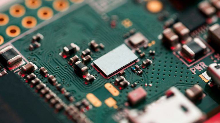
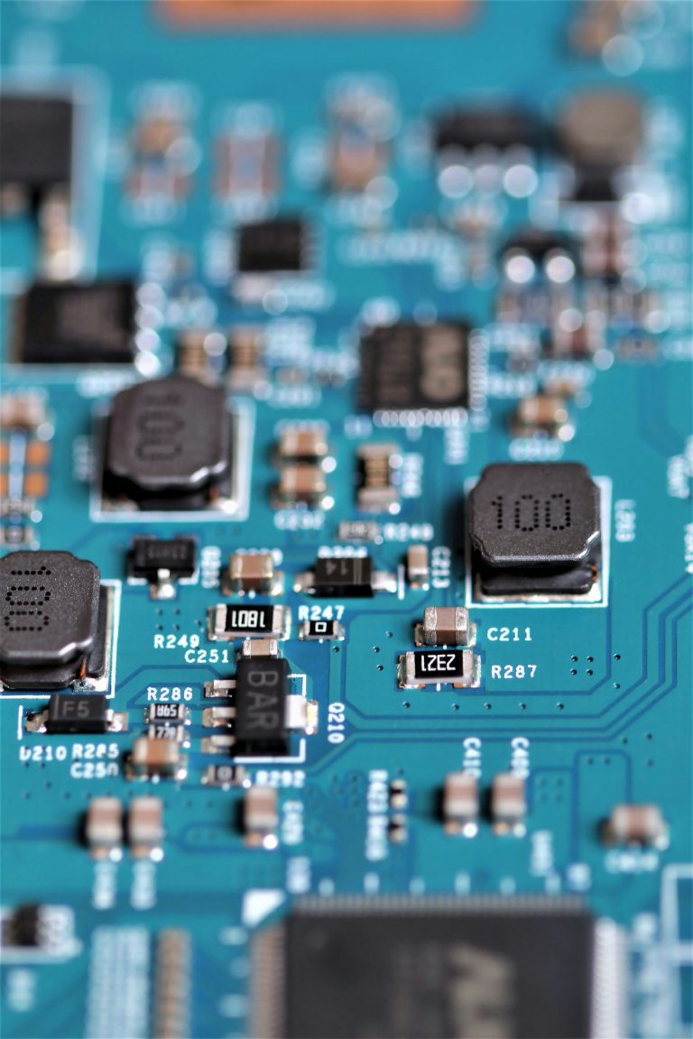
In high-speed and high-frequency PCB designs, surface finish is far more than a simple protective coating for bare copper. It directly governs signal integrity, insertion loss, impedance stability, solderability, oxidation resistance, mechanical durability, and long-term operational reliability. Driven by the skin effect, high-frequency electrical signals travel primarily along the outer surface of copper traces instead of the full copper cross-section. This makes the material composition, layer thickness, magnetic property, surface roughness, and flatness of PCB surface finish decisive factors for high-speed circuit performance. Understanding high speed pcb surface finish is essential for signal integrity.
The PCB Manufacturing & Testing Guidelines, which covers all manufacturing processes from prototype to mass production, provides essential context for understanding surface finish options. This in-depth pillar content integrates industry authoritative standards, manufacturing practice data, high-frequency loss analysis, and real engineering application cases. It fully elaborates the definition, working mechanism, classification, structural principle, pros and cons, technical parameters, failure risks, and scenario-based selection of mainstream high-speed PCB surface finishes including ENIG, ENEPIG, OSP, immersion silver, immersion tin, and hard gold plating.
Table of Contents
- 1. What Is PCB Surface Finish & Why It Matters for High-Speed PCB
- 2. Skin Effect: The Core Reason Surface Finish Impacts High-Speed Signal
- 3. Overview of Mainstream High-Speed PCB Surface Finish Types
- 4. ENIG: Structure, Performance & Application
- 5. ENEPIG: Premium High-Reliability Finish
- 6. OSP: Low-Cost Eco-Friendly Option
- 7. Immersion Silver & Immersion Tin: Low-Loss Comparison
- 8. Hard Gold Plating: Dedicated for PCB Gold Fingers
- 9. Comprehensive Comparison Table of All Surface Finishes
- 10. Quick Selection Guide by Application Scenario
- 11. Common Defects & Failure Risks
- 12. Key Takeaways
- 13. FAQ About High-Speed PCB Surface Finish
- 14. Get Professional Surface Finish Recommendation & PCB Quotation
What Is PCB Surface Finish & Why It Matters for High-Speed PCB
PCB surface finish refers to a thin protective layer deposited or chemically coated on exposed bare copper pads and traces after PCB etching and before SMT assembly. It acts as the critical interface between copper circuitry, electronic components, solder paste, connectors, and the external operating environment.
Core Functions of PCB Surface Finish
- Prevent bare copper from oxidation and sulfidation in air, avoiding non-conductive oxide layers
- Maintain stable and long-term solderability for reflow soldering and wave soldering
- Provide smooth, flat, and consistent pad surface for fine-pitch component mounting
- Offer durable conductive contact surface for gold finger plug-and-play interfaces
- Improve chemical corrosion resistance and environmental adaptability of PCBs
For conventional low-speed PCBs, surface finish only needs to meet basic soldering and anti-oxidation demands. But for high-speed PCB, RF, microwave, AI server, 5G baseband, and high-speed backplane circuits, surface finish becomes a core design factor. Unsuitable high speed pcb surface finish will cause excessive insertion loss, signal distortion, impedance fluctuation, crosstalk, and even system instability. The Signal Integrity Guide, which explains how material properties affect signal quality, provides essential background for understanding surface finish impacts. Choosing the right finish is the first step to guarantee high-speed signal integrity.
Skin Effect: The Core Reason Surface Finish Impacts High-Speed Signal
The skin effect is the fundamental physical principle why surface finish dominates high-speed PCB performance. At high frequencies, AC signals no longer flow evenly through the entire cross-section of copper traces. Instead, they concentrate on a thin outer “skin” layer of the copper surface. The higher the frequency, the thinner the signal penetration depth. This means high-speed signals almost entirely transmit on the contact interface between copper and surface finish.
Key influencing factors brought by surface finish:
- Magnetic permeability of plating material causes extra high-frequency loss
- Coating thickness changes surface roughness and impedance consistency
- Material conductivity directly determines insertion loss magnitude
- Flatness affects solder printing and component coplanarity for BGA/QFN
The Impedance Matching Ultimate Guide, which covers impedance control principles and tolerance guidelines, provides essential background for understanding how surface finish affects signal integrity. All high speed pcb surface finish selection must be based on skin effect and high-frequency loss characteristics.
Overview of Mainstream High-Speed PCB Surface Finish Types
There are six mainstream surface finishes widely used in high-speed and high-frequency PCB manufacturing:
- ENIG: Most popular balanced option, flat surface, good oxidation resistance
- ENEPIG: Upgraded three-layer structure, low black pad risk, wire bonding compatible
- OSP: Organic non-metal coating, lowest cost, negligible high-frequency loss
- Immersion Silver: Ultra-low high-frequency insertion loss, smooth surface
- Immersion Tin: Uniform flat coating, good solderability, tin whisker risk
- Hard Gold Plating: High hardness and wear resistance, for gold finger only
ENIG: Structure, Performance & Application
Layer Structure: Nickel barrier layer (3–6 μm) + Immersion gold top layer (0.05–0.1 μm). The nickel layer blocks copper diffusion; the thin gold layer provides permanent anti-oxidation and stable solderability.
Advantages: Ultra-flat surface, perfect for fine-pitch BGA and QFN. Excellent oxidation resistance and long storage cycle. Compatible with multiple reflow processes. Follows IPC-4552B standards.
High-Speed Performance: Nickel layer is non-ferromagnetic and will not cause severe magnetic loss. However, compared with immersion silver, ENIG still brings slightly higher insertion loss at 10GHz and above.
Suitable Applications: General high-speed PCB, server motherboard, industrial control high-speed board, consumer electronics high-speed module, BGA dense layout design. This is the most common high speed pcb surface finish for general applications.
ENEPIG: Premium High-Reliability Finish
Layer Structure: Electroless Nickel → Electroless Palladium → Immersion Gold. The added palladium layer acts as an enhanced barrier to isolate nickel corrosion and copper-gold diffusion.
Core Advantages: Fundamentally reduce black pad defect risk. Perfect compatibility with gold wire and aluminum wire bonding. Higher surface hardness and wear resistance. Stable performance under high temperature, humidity and long-term aging.
Cost & Positioning: ENEPIG cost is 1.5–2 times of standard ENIG. Not cost-effective for ordinary commercial PCBs, but irreplaceable for high-reliability scenarios.
Suitable Applications: Aerospace, military electronics, medical precision equipment, automotive high-reliability PCB, communication base station core board, projects requiring both wire bonding and gold finger function. For BGA-heavy designs requiring high reliability, the BGA Fanout Techniques guide provides additional layout recommendations that complement ENEPIG’s flat surface advantages.
OSP: Low-Cost Eco-Friendly Option
Working Principle: OSP forms an ultra-thin organic protective film on bare copper through chemical reaction. The organic layer volatilizes rapidly during high-temperature reflow, exposing fresh pure copper for solder wetting.
Advantages: Lowest cost among all finishes. Ultra-thin film brings almost zero impact on high-frequency insertion loss. Lead-free and environmentally friendly.
Limitations: Short shelf life (only 6 months under sealed dry storage). Cannot support multiple reflow cycles (only 1–2 times). Not applicable for gold finger contact and ultra-fine pitch BGA.
Suitable Applications: Cost-sensitive high-speed projects without BGA packaging, single reflow assembly, short storage cycle requirement.
Immersion Silver & Immersion Tin: Low-Loss Comparison
Immersion Silver
Electrical Performance: Highest conductivity, ultra-low insertion loss; 10GHz loss is 5%–20% lower than ENIG. Surface Feature: Extremely smooth and flat, excellent impedance stability. Shelf Life: 12–18 months. Hidden Risk: Silver electromigration under long-term humidity and biased voltage. Best For: RF circuit, microwave, millimeter-wave, ultra-high-speed differential signal board.
Immersion Tin
Electrical Performance: Medium high-frequency loss, not recommended for above 1GHz high-speed design. Shelf Life: 6–12 months. Hidden Risk: Serious tin whisker growth risk, micro short circuit on dense traces. Best For: Ordinary connector crimping board, conventional non-high-speed PCB.
For ultra-high-frequency RF designs, immersion silver is the optimal high speed pcb surface finish choice due to its minimal insertion loss.
Hard Gold Plating: Dedicated for PCB Gold Fingers
Layer Structure: Nickel barrier layer (4–6 μm) + Hard gold alloy layer (0.5–2 μm). Alloy doping improves gold hardness and friction resistance.
Core Features: Support 500+ times repeated insertion and extraction without obvious wear. Excellent mechanical wear resistance and oxidation resistance.
Limitations: Thick plating causes uneven surface, not suitable for high-speed signal traces. Gold brittleness leads to poor solder joint strength, not for reflow soldering.
Application Rule: High-speed PCB with both signal pads and gold fingers must adopt separate processing: ENIG or immersion silver for signal pads, dedicated hard gold plating for gold finger area.
Comprehensive Comparison Table of All Surface Finishes
| Surface Finish | Flatness | High-Freq Loss | Shelf Life | Reflow Times | Wear Resistance | Cost | Best For |
|---|---|---|---|---|---|---|---|
| ENIG | Excellent | Medium | Long | Multiple | Medium | Medium | General high-speed, BGA |
| ENEPIG | Excellent | Medium | Ultra-Long | Multiple | Excellent | Very High | Military, medical, wire bond |
| OSP | Good | Negligible | Short | 1–2 | Low | Very Low | Cost priority, no BGA |
| Immersion Silver | Excellent | Low | Long | Multiple | Medium | Med-High | RF, microwave, ultra-high freq |
| Immersion Tin | Good | Medium | Short | 1–2 | Low | Low | Connector board |
| Hard Gold | Fair | High | Ultra-Long | Not for reflow | Excellent | High | Gold finger plug-in |
Quick Selection Guide by Application Scenario
| Application Scenario | Recommended Surface Finish |
|---|---|
| General high-speed PCB with BGA/QFN | ENIG |
| High-end projects needing wire bonding + gold finger | ENEPIG |
| RF, microwave, 5G/6G, millimeter-wave | Immersion Silver |
| Cost-sensitive, no BGA, single assembly, short storage | OSP |
| PCB with frequent plug-and-play gold finger | Hard Gold for fingers + ENIG for pads |
| Conventional non-high-speed connector board | Immersion Tin |
Common Defects & Failure Risks
| Defect | Affected Finish | Cause & Prevention |
|---|---|---|
| Black Pad | ENIG | Nickel corrosion; ENEPIG avoids it |
| Tin Whisker | Immersion Tin | Spontaneous crystal growth; avoid for dense traces |
| Silver Electromigration | Immersion Silver | Humid environment; not for high-voltage dense pads |
| OSP Film Failure | OSP | Humidity exposure; control storage conditions |
| Gold Brittleness | Hard Gold | Poor solder joints; not for reflow soldering |
All risks can be avoided by selecting correct high speed pcb surface finish and following IPC manufacturing standards.
Key Takeaways
- High speed pcb surface finish selection cannot only focus on cost; skin effect and high-frequency insertion loss must be prioritized
- ENIG is the universal first choice for most commercial and industrial high-speed PCB designs
- For ultra-high-frequency RF and low-loss sensitive circuits, immersion silver is optimal
- Gold finger interface must use dedicated hard gold plating; ENIG is not suitable
- ENEPIG is the premium high-reliability option for aerospace, medical and military projects
- OSP is only suitable for cost-sensitive simple high-speed boards with no fine-pitch components
FAQ About High-Speed PCB Surface Finish
Q1: Which surface finish has the lowest insertion loss for high-speed PCB?
Immersion silver has the lowest high-frequency insertion loss, followed by OSP; ENIG and ENEPIG are medium loss, while hard gold has the highest loss. This is a key consideration for high speed pcb surface finish selection.
Q2: Is ENIG suitable for 10GHz and above high-frequency design?
Yes for most general scenarios; for strict low-loss millimeter-wave circuits, immersion silver is better.
Q3: What is the difference between ENIG and ENEPIG?
ENEPIG adds a palladium layer, lower black pad risk, supports wire bonding, higher wear resistance, but costs 1.5–2 times more than ENIG.
Q4: Can OSP be used for BGA high-speed PCB?
Not recommended. OSP flatness and reflow resistance cannot meet fine-pitch BGA assembly requirements.
Q5: How long is the shelf life of ENIG PCB?
Under standard vacuum dry packaging, ENIG can be stored for 12 months or longer without obvious oxidation.
Q6: Why can’t hard gold be used for normal soldering pads?
Hard gold has gold brittleness, poor solder joint mechanical strength, and uneven surface affecting impedance and signal integrity.
Get Professional Surface Finish Recommendation & PCB Quotation
Choosing the wrong high speed pcb surface finish for your project will lead to signal loss, assembly yield drop, oxidation failure or extra cost waste. If you are unsure which finish fits your frequency range, component type, assembly process, working environment and budget, our professional high-speed PCB engineering team can provide one-to-one customized surface finish recommendation.
We offer: Free surface finish selection consulting • Signal integrity analysis • Solderability and reliability evaluation • Competitive PCB manufacturing quotation
Submit your PCB design files, frequency parameters and application requirements through our inquiry form. We will reply with professional technical suggestions and competitive manufacturing quotation within the shortest time.
About HighSpeedPCBs.com
We are a specialized PCB design and manufacturing service provider serving industrial, automotive, medical, and communications OEMs worldwide. Complete manufacturing process documentation, including detailed surface finish specifications, is available in the PCB Manufacturing & Testing Guidelines. Our expertise in high speed pcb surface finish selection ensures your high-speed designs achieve optimal signal integrity.
© 2026 HighSpeedPCBs.com — Professional High-Speed PCB Solutions