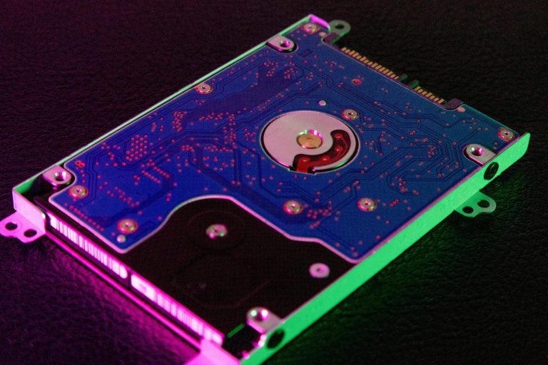
High-speed PCB design and manufacturing differ drastically from standard rigid PCBs, requiring strict control over layer structure, fine-line routing, microvia precision, special processes, low-loss materials and impedance stability. Understanding high speed pcb manufacturing capability is essential for successful project delivery. Choosing a PCB manufacturer without verifying real production capability often leads to design rework, production scrap, delivery delays and signal integrity failures.
This pillar content consolidates industry top manufacturer standards, Altium DFM engineering guidelines and high-volume mass-production criteria, delivering a one-stop, fully structured high speed pcb manufacturing capability guide. You will get clear parameter comparisons, professional process explanations, a practical supplier evaluation checklist, DFM best practices and common FAQs — ideal for hardware engineers, procurement managers and supply chain buyers to screen qualified high-speed PCB vendors and avoid manufacturability risks. Mastering high speed pcb manufacturing capability evaluation is the first step to reliable production.
Complete manufacturing process documentation is available in PCB Manufacturing & Testing, which covers all processes from prototype to mass production. This high speed pcb manufacturing capability guide focuses specifically on supplier evaluation within that framework.
Table of Contents
- 1. What Is High-Speed PCB Manufacturing Capability & Why It Matters
- 2. Basic Structural & Fabrication Capability Parameters
- 3. HDI & Microvia Drilling Manufacturing Capabilities
- 4. Special High-Speed Process Capabilities: Back Drilling, Impedance Control & More
- 5. High-Speed PCB Substrate Materials & Hybrid Lamination Capability
- 6. Surface Finish Options for High-Speed PCBs
- 7. Testing, Inspection & Reliability Qualification Capability
- 8. Step-by-Step High-Speed PCB Supplier Capability Checklist
- 9. Key Takeaways & DFM Best Practices
- 10. FAQ About High-Speed PCB Manufacturing Capability
- 11. Get Free Design Review & PCB Manufacturing Quotation
What Is High-Speed PCB Manufacturing Capability & Why It Matters
High speed pcb manufacturing capability refers to a PCB factory’s stable, repeatable mass production process window, including structural limits, precision craftsmanship, material compatibility, electrical control accuracy and full reliability testing standards. It is not just the lab-level extreme parameters, but the consistent yield and batch stability that matters for commercial, industrial, telecom and aerospace applications. Evaluating high speed pcb manufacturing capability requires looking beyond marketing claims.
Unlike conventional PCBs, high-speed circuits running at 1Gbps to 100Gbps are extremely sensitive to transmission loss, impedance fluctuation, via stub resonance, layer misalignment and material dielectric performance. If your design exceeds the supplier’s actual high speed pcb manufacturing capability, common consequences include prototype and mass production scrap, multiple design iterations and delayed project timelines, uncontrolled impedance causing signal integrity issues, poor thermal performance and short product service life, and higher hidden costs from rework and order replacement.
For design engineers, hardware teams and international procurement buyers, mastering high speed pcb manufacturing capability evaluation is the first step of DFM. This guide standardizes all core evaluation dimensions, helping you match your design stackup, routing density and special process requirements with qualified manufacturers accurately. A thorough high speed pcb manufacturing capability assessment prevents costly downstream failures.
Detailed HDI structures that require advanced capability are covered in HDI PCB Manufacturing, which explains stackup options for any-layer designs that push the boundaries of high speed pcb manufacturing capability.
Basic Structural & Fabrication Capability Parameters
Basic manufacturing parameters form the foundation of all high-speed PCB projects. Every professional supplier must provide documented standard and advanced capability ranges, covering layer count, line/space width, board thickness and maximum panel size. These baseline metrics are the first indicators of high speed pcb manufacturing capability.
| Parameter | Standard Capability | Advanced Capability | Practical Note |
|---|---|---|---|
| Maximum Layer Count | 20–24 Layers | 32–40 Layers+ | Server backplanes, 5G base stations, AI computing |
| Minimum Line / Space | 4/4 mil | 3/3 mil, 2/2 mil | Finer trace increases density but raises cost |
| Board Thickness | 0.4mm – 3.2mm | 3.2mm – 6.0mm | Thin wearable to thick industrial backplanes |
| Maximum Panel Size | 500×600mm | 600×800mm+ | Larger panels improve material utilization |
Maximum layer capacity determines whether complex stackup designs can be produced stably. Standard 20–24 layers fit most industrial and consumer high-speed products, while advanced 32–40+ layer capability is mandatory for high-end server and telecom hardware. These parameters directly reflect a supplier’s high speed pcb manufacturing capability and should be verified before engagement.
HDI & Microvia Drilling Manufacturing Capabilities
HDI (High Density Interconnect) technology is indispensable for modern miniaturized high-speed PCBs. Microvia drilling precision, aspect ratio control and HDI stack structure directly affect signal path length, transmission loss and component layout density. A supplier’s HDI expertise is a key component of high speed pcb manufacturing capability.
| HDI Parameter | Standard Capability | Advanced Capability |
|---|---|---|
| Minimum Laser Microvia | 0.1mm | 0.075mm |
| Minimum Mechanical Hole | 0.2mm | 0.15mm |
| Maximum Aspect Ratio | 10:1 | 15:1 |
| Supported HDI Structure | 1+N+1 | 2+N+2, Any-layer |
Laser drilling defines ultra-fine microvias for fine-pitch packaged devices. Advanced factories use high-precision laser equipment to achieve 0.075mm microvias, supporting ultra-compact high-speed module designs. Aspect ratio reflects the factory’s plating quality and hole-wall reliability; a higher ratio ensures no cracking or copper voids in thick multilayer boards. Any-layer HDI allows arbitrary interlayer connection, optimizing high-speed signal return paths and reducing parasitic noise — essential for 25Gbps+ high-speed differential circuits and advanced high speed pcb manufacturing capability. Back drilling requirements that often accompany HDI structures are covered in Back Drilling Process.
Special High-Speed Process Capabilities: Back Drilling, Impedance Control & More
Standard PCB processes cannot meet high-speed signal demands. Special process capability is the core competitiveness that separates ordinary PCB factories from professional high-speed manufacturers. These advanced processes define true high speed pcb manufacturing capability.
| Special Process | Standard Level | Advanced High-Speed Level |
|---|---|---|
| Back Drilling Depth Tolerance | ±0.1mm | ±0.05mm |
| Impedance Control Tolerance | ±10% | ±7% / ±5% |
| Via Plugging Technology | Resin Plug Hole | Copper Plug Hole |
| Embedded Resistor / Capacitor | Not Supported | Fully Supported |
Back drilling removes redundant via stubs that cause signal reflection and resonance. For 10Gbps+ SerDes signals, only ±0.05mm tight tolerance can ensure signal integrity. Design-side impedance calculations are covered in Impedance Matching Ultimate, which complements the manufacturing focus here. Impedance control is the most critical index for high-speed PCBs. Standard ±10% tolerance suits non-critical routes; high-frequency RF and high-speed interface circuits require ±5% precision with TDR testing on every production panel — a hallmark of superior high speed pcb manufacturing capability.
High-Speed PCB Substrate Materials & Hybrid Lamination Capability
PCB substrate material determines dielectric constant (Dk), loss tangent (Df), thermal stability and high-frequency transmission loss. A qualified high-speed supplier must support full material grades and mature hybrid lamination technology. Material compatibility is a cornerstone of high speed pcb manufacturing capability.
- Standard FR4 / High Tg FR4: Basic material for general high-speed designs, good thermal resistance and cost efficiency
- Rogers / Isola / Megtron: Low-loss high-speed materials for 10GHz+ high-frequency and server applications; must confirm factory stock and certified lamination process
- Hybrid Lamination (FR4 + High-Speed Material): Balances electrical performance and cost, widely used in communication hybrid modules
- PTFE High-Frequency Material: Ultra-low loss for millimeter-wave RF designs, requiring customized drilling, pressing and plating workflows
When auditing suppliers, do not only check material brand support — verify whether they have stable batch lamination experience, controlled Dk/Df deviation and long-term aging stability data. Material properties that affect high-speed performance — analyzed in PCB Materials Selection — provide essential context for high speed pcb manufacturing capability assessment.
Surface Finish Options for High-Speed PCBs
Surface finish impacts solderability, oxidation resistance, high-frequency electrical performance and product service life. High-speed PCB projects should select plating based on frequency requirement, cost and assembly process. Surface finish selection is an integral part of high speed pcb manufacturing capability.
- ENIG: Universal finish with flat surface, suitable for high-density BGA soldering
- ENEPIG: Best high-frequency performance, ideal for premium high-speed and RF circuits
- OSP: Cost-effective, good for large-batch consumer high-speed products
- Immersion Silver: Stable conductivity for precision high-speed analog and digital mixed circuits
Professional manufacturers can recommend the most cost-effective surface finish according to your application scenario. A full comparison of all finishes — available in Surface Finish for High-Speed PCB — helps you select the optimal plating for your frequency range and confirms the supplier’s high speed pcb manufacturing capability in this area.
Testing, Inspection & Reliability Qualification Capability
Paper process parameters are meaningless without complete testing and reliability verification. Reliable high-speed PCB suppliers must equip standardized inspection and test systems. Comprehensive testing validates high speed pcb manufacturing capability in production.
- Flying Probe Test: Standard open/short circuit detection for every board
- TDR Impedance Test: Exclusive for high-speed PCBs to verify actual impedance matching design targets
- X-Ray Inspection: Non-destructive check for buried vias, BGA hidden joints and layer alignment
- Microsection Analysis: Sampling inspection of hole-wall plating, lamination quality and resin uniformity
- Thermal Cycle & CAF Testing: For automotive, aerospace and industrial high-reliability projects
Only manufacturers with complete testing workflows can guarantee batch consistency and long-term reliability for high-speed products. TDR testing, in particular, is mandatory for verifying high speed pcb manufacturing capability on controlled impedance designs.
Step-by-Step High-Speed PCB Supplier Capability Checklist
Use this checklist to evaluate any high-speed PCB supplier’s high speed pcb manufacturing capability item by item, eliminating information asymmetry and DFM risks:
- Confirm maximum layer count matches your stackup with reasonable process margin
- Verify minimum line/space capability fits routing density and budget expectation
- Confirm HDI structure, laser aperture and aspect ratio meet BGA layout requirements
- Clarify back drilling tolerance, impedance accuracy and via plugging process standards
- Check designated high-speed material brand availability, stock and lamination maturity
- Ensure the supplier provides official TDR test reports and batch inspection data
- Request full manufacturing capability specification documents and industry qualification certificates
- Confirm lead time, mass-production yield and engineering DFM support availability
Key Takeaways & DFM Best Practices
- Never only reference a factory’s extreme lab parameters — prioritize mass-production stability and yield when evaluating high speed pcb manufacturing capability
- Confirm material, HDI structure and special processes at the early design stage, not after layout completion, to ensure high speed pcb manufacturing capability alignment
- Reserve sufficient tolerance for line width, aperture, impedance and layer alignment to reduce production difficulty
- Match surface finish and testing standards according to your product application, avoiding unnecessary cost waste
- Choose suppliers with professional DFM engineering support and proven high speed pcb manufacturing capability, not only manufacturing capacity
FAQ About High-Speed PCB Manufacturing Capability
Q1: What is the biggest difference between standard PCB and high-speed PCB manufacturing capability?
High-speed PCB requires strict impedance control, low-loss material matching, precise back drilling, microvia HDI capability and professional TDR testing — this defines true high speed pcb manufacturing capability and separates advanced suppliers from basic PCB manufacturers.
Q2: Is ±10% impedance tolerance enough for high-speed design?
Only for low-to-medium speed signals. For 10Gbps+ differential lines and RF circuits, ±5%~±7% tolerance is strongly recommended as part of robust high speed pcb manufacturing capability.
Q3: What is Any-layer HDI used for?
It enables free interlayer connection, shorter signal paths, lower loss and is widely used in server, AI board and high-end communication hardware requiring advanced high speed pcb manufacturing capability.
Q4: How to quickly judge if a supplier is qualified for high-speed PCBs?
Check their layer capacity, fine-line capability, HDI parameters, impedance tolerance, high-speed material support and complete testing system — all part of high speed pcb manufacturing capability assessment.
Q5: What testing is mandatory for high-speed PCBs?
TDR impedance testing is mandatory for all controlled impedance designs; flying probe, X-ray and microsection are also required for quality assurance in high speed pcb manufacturing capability verification.
Get Free Design Review & PCB Manufacturing Quotation
Do you have finished high-speed PCB design files and want to verify manufacturability, check process compatibility, confirm cost and lead time? Our team specializes in high speed pcb manufacturing capability assessment and matching.
We offer: Free DFM review • High speed pcb manufacturing capability matching • Material recommendation • Stackup check • Customized quotation
Submit your PCB design files and project requirements now to get a no-obligation professional evaluation and factory-matched manufacturing quote.
About HighSpeedPCBs.com
We are a specialized PCB design and manufacturing service provider serving industrial, automotive, medical, and communications OEMs worldwide. Complete manufacturing process documentation is available in PCB Manufacturing & Testing. Our expertise in high speed pcb manufacturing capability ensures your high-speed designs are manufacturable and reliable.
© 2026 HighSpeedPCBs.com — Professional High-Speed PCB Solutions