Article Abstract
Signal reflection is one of the most common and damaging signal integrity problems in high-speed PCB design. It occurs when electrical signals hit impedance discontinuities along transmission lines, causing energy to bounce back toward the source. The result is distorted waveforms: overshoot, undershoot, ringing, and stepped edges that lead to timing errors, false logic switching, EMI radiation, and even component damage.
This complete guide explains the fundamental theory of PCB reflection issues, lists clear visible symptoms, breaks down all root causes, introduces professional troubleshooting tools like TDR, oscilloscope, and VNA, provides practical repair solutions, shares a step-by-step troubleshooting workflow, and offers a ready-to-use design prevention checklist. We also include frequently asked questions and professional engineering support for your high-speed PCB projects. Suitable for hardware engineers, layout designers, and global PCB procurement buyers.
1. Signal Reflection – When High-Speed Signals Bounce Back
Signal reflection is a fundamental transmission line phenomenon in high-speed printed circuit boards. As detailed in the High-speed PCB troubleshooting master page, reflection is one of the most common signal integrity failures. Whenever a propagating electrical signal encounters any impedance discontinuity on its path, part of the signal energy cannot continue forward and reflects back to the driver source end. The superposition of incident waves and reflected waves distorts the original clean waveform and destroys signal integrity.
In low-speed circuit designs, trace length is far shorter than the signal rise time wavelength, and reflection effects can be ignored. However, for modern high-speed interfaces such as DDR4/DDR5, PCIe, USB4, and HDMI, even minor impedance changes will trigger obvious reflection interference. Understanding PCB reflection issues is essential for any hardware engineer.
Typical visible performances include overshoot, undershoot, continuous ringing, and slow stepped rising edges. These anomalies easily cause system instability, timing margin shrinkage, electromagnetic interference failure, and long-term device latch-up damage. For related signal integrity problems, see PCB impedance issues.
The most common triggers in actual PCB layouts include sudden trace width changes, unused via stubs, long unterminated branch stubs, mismatched connectors, split reference planes, and missing terminal resistance matching.
2. Clear Symptoms of PCB Reflection Problems
Reflection generates highly recognizable waveform features that engineers can quickly identify with an oscilloscope or eye diagram analysis. Each symptom corresponds to different failure mechanisms and severity levels, allowing fast preliminary judgment. Recognizing these PCB reflection issues early saves significant debugging time.
Overshoot – The signal voltage exceeds the normal high logic level with an abnormally high first peak. Medium to high severity. It may exceed the maximum rated voltage of chips, cause gate breakdown and irreversible component damage.
Undershoot – The signal drops far below the standard low logic threshold with an obvious negative valley. Medium to high severity. It easily triggers false switching of sensitive logic circuits and increases susceptibility to external noise coupling.
Ringing – Repeated up-and-down oscillation after signal edge transition, forming multiple round-trip bounces. High severity. It prolongs settling time, compresses timing margins, and greatly increases EMI radiation.
Stepped Waveform – The rising or falling edge presents a slow stair-step shape instead of a smooth transition. Medium severity. Usually caused by multiple weak impedance discontinuities or long stubs, mainly affecting parallel bus synchronization.
Eye Diagram Distortion – The upper and lower boundaries of the eye mask expand abnormally, eye opening shrinks, and bit error rate rises. Medium severity. Common in high-speed serial links and directly limits maximum operating frequency.
Comparing standard and distorted waveforms is the fastest way for engineers to confirm whether signal anomalies come from reflection rather than crosstalk or power noise. For PCB crosstalk issues, see the separate troubleshooting guide.
3. Root Causes of Signal Reflection on PCBs
All PCB reflection issues stem from one core reason: intermittent characteristic impedance inconsistency. Any design structure, layout method or manufacturing deviation that breaks impedance continuity will produce reflected waves. The main root causes are summarized as follows:
Impedance Mismatch from Trace Width Changes – Abrupt trace width modification changes the copper cross-sectional area and the distance to the reference plane, forming local impedance spikes or dips.
Unoptimized Via Stubs – Through-hole vias often leave unused copper barrel segments beyond the connection layer, forming via stubs. These stubs are equivalent to miniature resonant transmission lines, generating strong reflection at specific frequencies.
Long Branch Traces and T-Junction Stubs – Unreasonable layout creates T-junctions and overly long unterminated branches. Signals reflect back and forth between the main line, branch end and driver, forming superposed multiple reflections.
Mismatched Connectors – Board-to-board and high-speed interface connectors differ in internal structure, dielectric material and pin pitch from PCB traces. The inherent impedance discontinuity at the connector interface directly causes partial signal reflection.
Missing or Improper Termination – Without source-series or load-parallel termination, the signal encounters approximate open-circuit or short-circuit conditions at the line end, producing full energy reflection.
Split Reference Planes – When high-speed traces cross gaps in ground or power planes, return current must detour around the split area. The increased loop inductance creates sudden impedance peaks, triggering reflection while worsening crosstalk and EMI. Proper Return Path design is essential to prevent these issues.
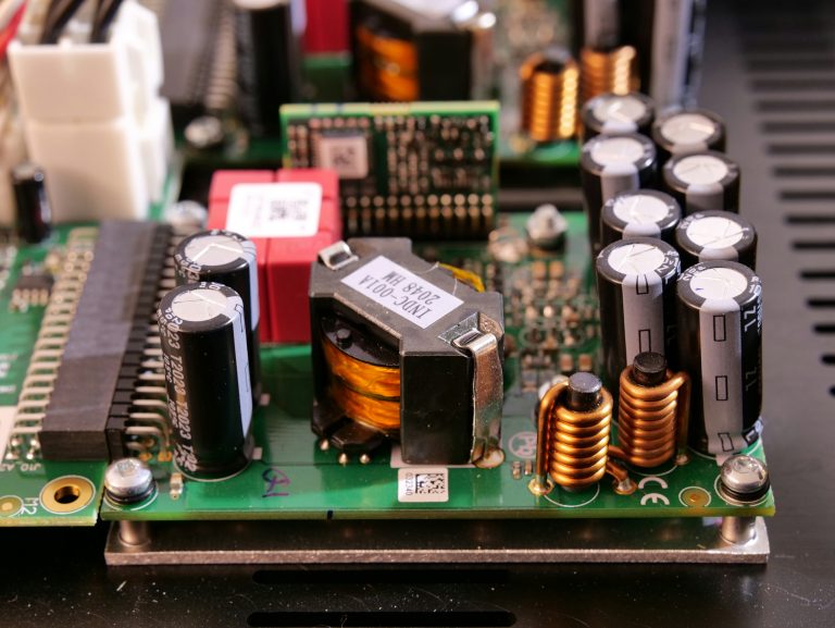
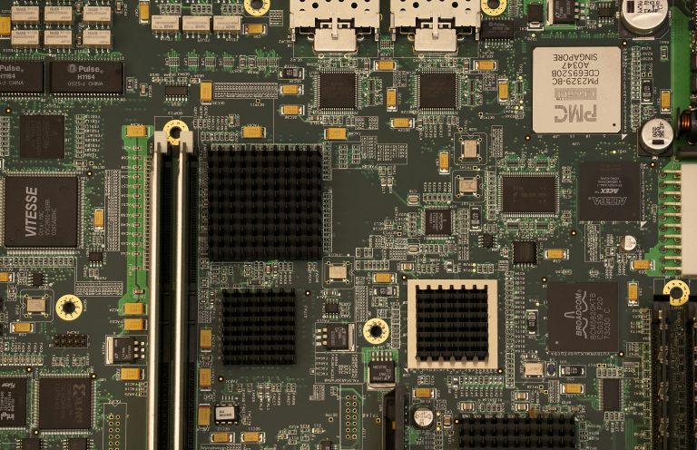
Manufacturing Tolerance Deviation – Actual PCB production errors such as etching deviation, dielectric thickness tolerance and copper thickness inconsistency will cause impedance drift beyond the standard ±10% range. For PCB Manufacturing, tight process control is critical.
4. Locate Reflection Points with TDR, Oscilloscope and VNA
Observing waveform distortion is not enough; engineers must accurately locate the specific physical position of impedance discontinuity. Four mainstream professional methods cover design simulation, prototype testing and mass production verification.
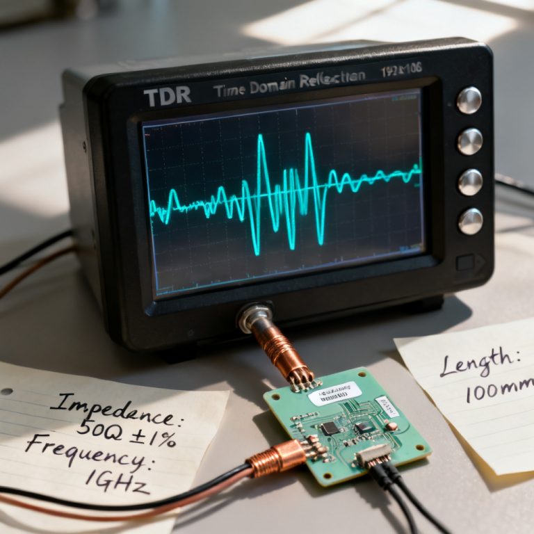
TDR (Time Domain Reflectometry) – TDR is the most professional tool for reflection positioning. It injects a fast step pulse into the transmission line and calculates the exact position and impedance value of the discontinuity through the time and amplitude of the reflected wave. It reaches sub-inch high precision and can quickly locate via stubs, trace width changes, connector boundaries and plane splits.
High-Bandwidth Oscilloscope – Used to capture real-time signal edges and identify overshoot, undershoot and ringing. Although it cannot locate specific reflection positions, it can quickly screen whether waveform anomalies are caused by reflection.
VNA (Vector Network Analyzer) – VNA tests return loss and insertion loss in the full frequency domain, quantifying reflection intensity at different working frequencies.
Time-Domain SI Simulation – Performed in the pre-layout and post-layout design stage. By modeling trace length, via structure, stub length and termination scheme, engineers can predict potential reflection risks in advance.
5. Effective Solutions to Fix PCB Reflection Issues
Corresponding targeted solutions can be adopted according to different reflection causes, with clear applicable scenarios and optimization effects. Addressing PCB reflection issues requires a multi-pronged approach.
Series Source Termination – Add a series resistor near the driver end to match the chip output impedance with the transmission line characteristic impedance. Suitable for point-to-point high-speed signals, effectively suppressing initial overshoot.
Parallel & AC Load Termination – Install pull-up, pull-down or RC termination at the load end to absorb residual signal energy and eliminate terminal full reflection. Ideal for multi-load high-speed buses.
Via Back Drilling – Remove redundant copper barrels of through-hole vias to completely eliminate resonance reflection caused by stubs. It is the most effective solution for high-layer high-speed PCBs.
Stub Removal and Layout Optimization – Redesign routing paths, shorten T-junction branches, and cancel unnecessary long stubs to avoid multiple superposed reflections.
Via Structure Optimization – Optimize via pad size, anti-pad clearance and hole diameter to maintain impedance continuity during layer switching.
Gradual Trace Width Transition – Use smooth gradient wiring instead of abrupt width changes to realize slow impedance transition.
Laminate and Material Upgrade – For high-frequency high-precision scenarios, adopt low Df, low dielectric loss high-Tg materials and standardized stacked layers to control impedance tolerance within ±10%. For High-Speed PCB Material, proper selection is critical.
6. Step-by-Step PCB Reflection Troubleshooting Flow
Follow this standardized five-step process to efficiently troubleshoot PCB reflection issues without blind modification:
Step 1: Capture and Analyze Waveforms – Use a high-bandwidth oscilloscope to capture abnormal edges, confirm overshoot, undershoot or ringing, and exclude interference from crosstalk and power ripple.
Step 2: Precise Positioning with TDR – Carry out TDR testing on problematic nets to mark the exact physical position of impedance discontinuity.
Step 3: Classify Root Causes – Determine whether the fault comes from impedance mismatch, via stubs, branch lines, connector mismatch, missing termination or cross-plane routing.
Step 4: Select Targeted Fix Scheme – Match corresponding solutions: add termination for impedance mismatch, adopt back drilling for via stubs, optimize layout for long branches.
Step 5: Modify, Retest and Verify – Complete layout optimization or prototype rework, then recheck waveforms via oscilloscope, TDR or VNA until signals meet SI and timing specifications.
7. High-Speed PCB Reflection Prevention Design Checklist
The best way to handle reflection is proactive design prevention. Follow this checklist during layout review to eliminate hidden risks in advance:
- Add reasonable source or load termination for all high-speed critical signals
- Strictly control T-junction and branch stub length, avoid long unterminated lines
- Apply back drilling for high-speed through-hole vias to remove redundant stubs
- Optimize via anti-pad and pad size to maintain layer-transition impedance continuity
- Control transmission line impedance tolerance within ±10%
- Forbid high-speed traces crossing split ground/power planes to keep complete return paths
- Prefer high-speed connectors with stable impedance parameters
- Adopt gradual transition for trace width changes instead of abrupt jumps
8. Key Takeaways
- PCB reflection issues are inevitable in high-speed design, and the core cause is impedance discontinuity on transmission lines
- Typical symptoms include overshoot, undershoot, ringing and stepped waveforms, which threaten system stability and timing margin
- Common root causes cover trace width mutation, via stubs, branch lines, mismatched connectors, missing termination and split reference planes
- TDR is the most efficient positioning tool, combined with oscilloscope, VNA and time-domain simulation
- Practical fixes include series/parallel termination, back drilling, stub removal, via optimization and gradient wiring
- Following the standardized troubleshooting process and design checklist can minimize reflection risks at the design stage
For a complete understanding of all troubleshooting topics, return to the High-speed PCB troubleshooting master page.
9. FAQ About PCB Reflection Issues
Q1: What is the main cause of PCB signal reflection?
The fundamental cause is impedance discontinuity on transmission lines, including trace width changes, via stubs, branch lines, split planes and missing termination.
Q2: What damage will signal reflection cause?
It leads to overshoot/undershoot device stress, false logic triggering, timing margin reduction, serious ringing, increased EMI and high bit error rate in high-speed links.
Q3: How to quickly find reflection points on a finished PCB?
Use TDR testing for precise positioning; use an oscilloscope for preliminary waveform judgment and VNA for frequency domain reflection loss analysis.
Q4: Is termination the best way to fix reflection?
Termination is one of the most effective methods for point-to-point and multi-load signals. For via stub problems, back drilling is more targeted.
Q5: Can PCB manufacturing errors cause reflection?
Yes. Etching deviation, dielectric thickness variation and copper thickness error will lead to impedance drift and induce unexpected reflection.
10. Get Professional Help with Your PCB Reflection & SI Optimization
Are you struggling with unstable waveforms, overshoot ringing, timing failure or EMI certification issues on your high-speed PCB design? Do you need professional TDR analysis, signal integrity simulation, layout optimization or termination scheme customization?
Our professional engineering team provides one-stop PCB signal integrity services: reflection fault diagnosis, high-speed layout review, via stub optimization, back drilling design guidance, impedance control scheme and full SI simulation verification.
Whether you are in the schematic design stage, layout optimization stage or prototype debugging stage, we can provide tailored technical solutions to eliminate PCB reflection issues, improve system stability, and save your time and board revision costs.