Article Abstract
Controlled impedance is the backbone of high-speed PCB signal integrity. Uncontrolled or out-of-tolerance pcb impedance issues frequently trigger signal reflection, overshoot, undershoot, ringing, closed eye diagrams, and even intermittent system crashes or data transmission errors. These anomalies stem from three core dimensions: design calculation errors, substrate material dielectric constant deviation, and PCB manufacturing process drift.
Time Domain Reflectometry (TDR) serves as the industry-standard diagnostic tool to locate impedance discontinuities, measure actual impedance values, and identify systematic or local deviations. This comprehensive pillar guide integrates professional principles, symptom comparison tables, root cause classification, TDR working mechanisms, standardized troubleshooting workflows, design-level optimization strategies, and manufacturing-side rectification solutions. Suitable for hardware engineers, PCB designers, procurement specialists, and industrial electronic buyers, it balances professional depth with easy-to-understand logic, helping you quickly diagnose, resolve, and prevent pcb impedance issues out-of-tolerance problems.
Impedance Issues – A Leading Cause of Signal Integrity Failures
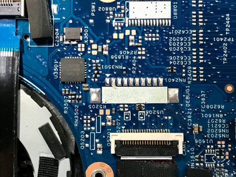
In modern high-speed digital circuits, automotive electronics, industrial control systems, and communication PCBs, PCB impedance issues rank as the most frequent root cause of signal integrity failures. As detailed in the High-speed PCB troubleshooting master page, understanding impedance is the first step in diagnosing signal integrity problems. Controlled impedance refers to maintaining a fixed characteristic impedance value of PCB transmission lines according to design requirements, usually controlled within ±10% tolerance for mass production.
Once the actual impedance deviates from the designed range, the signal cannot achieve energy matching between the source, transmission line, and load. The direct consequences include signal reflection, excessive overshoot and undershoot, continuous waveform ringing, distorted edge signals, and collapsed eye diagrams. Troubleshooting PCB impedance issues requires a systematic approach using TDR testing, especially critical in high-speed applications like SerDes PCB Design where 56G and 112G PAM4 signals have extremely tight timing margins.
Common Symptoms of PCB Impedance Issues (With Severity Guide)
Impedance mismatch always presents obvious test waveform and signal performance features. By identifying typical symptoms, engineers can quickly judge whether circuit abnormalities are caused by PCB impedance issues, instead of wasting time on power supply or component troubleshooting.
。Overshoot / Undershoot over 20%68
| Symptom | Direct Cause | Risk Severity |
|---|---|---|
| Actual impedance higher or lower than design value | Medium to High | |
| Continuous waveform ringing | Multiple reflections from impedance discontinuity points | High |
| Obvious step jumps on TDR curve | Local impedance discontinuity on traces, vias or pads | Medium |
| Narrowed or closed eye diagram | Superposition of impedance mismatch, reflection and line loss | High |
Overshoot and undershoot beyond 20% are the most intuitive early warnings. Excessively high impedance causes voltage overshoot, while low impedance leads to undershoot. Sustained ringing occurs when signals bounce repeatedly at discontinuous points. TDR curve jumps are the most reliable basis for locating local defects, such as sudden trace width changes and oversized via pads. For Ethernet PCB Design, impedance control is critical for 10G/25G/100G backplane channels.
Root Causes of PCB Impedance Issues (Design / Material / Manufacturing)
PCB impedance issues never come from a single factor. They run through design, material, and manufacturing links. For High-Speed PCB Material data, proper material choice is the first line of defense against impedance problems.
Design Level: Incorrect trace width calculation, unreasonable layer stackup, oversized via pads and anti-pads, ignoring reference plane segmentation.
Material Level: Dielectric constant (Dk) deviation, substrate material batch inconsistency, solder mask thickness variation.
Manufacturing Level: Over-etching or under-etching, uncontrolled lamination thickness, unstable copper foil thickness, process parameter random adjustment.
For PCB Manufacturing process control, ensure all lamination and etching parameters are locked. Many PCB impedance issues originate from manufacturing process drift rather than design errors.
How TDR Works & Why It Is the Standard Impedance Diagnosis Tool
Time Domain Reflectometry (TDR) is the most authoritative, intuitive, and efficient tool for troubleshooting PCB impedance issues, widely adopted for high-speed signal integrity analysis. TDR emits a fast rising-edge step pulse into the PCB transmission line. The signal propagates along the trace at a fixed speed. When it encounters any impedance discontinuous point, part of the signal energy is reflected back.
Core functions: Qualitative judgment (distinguish systematic offset vs local discontinuity), quantitative measurement (read real impedance values), precise positioning (mark exact fault locations). For USB PCB Design, TDR testing is recommended for USB4 high-speed lanes.
Step-by-Step PCB Impedance Issues Troubleshooting Workflow
Step 1: Review Design Documents – Check layer stackup, trace width settings, via pad dimensions. For PCIe PCB Design, pay special attention to AC coupling capacitor pad optimization.
Step 2: Conduct Professional TDR Measurement – Test all controlled impedance networks, record complete TDR curves.
Step 3: Microsection Slicing Verification – Select typical abnormal positions for blind slicing to verify actual trace width and dielectric spacing.
Step 4: Audit Factory Production Records – Check substrate Dk batch reports, lamination parameters, etching process logs.
Step 5: Implement Optimization & Re-Validation – Classify faults and launch targeted improvements. For AI server PCB design, where PCIe 5.0/6.0 channels demand tight impedance control, follow this workflow meticulously.
Design-Level Solutions to Fix PCB Impedance Issues
When PCB impedance issues originate from design flaws, optimizing at the design stage can fundamentally eliminate systematic failures:
Optimize layer stackup – Recalculate dielectric layer thickness with professional impedance simulation software.
Adjust trace width and transition layout – Modify controlled impedance trace width according to actual substrate Dk; avoid sudden trace width changes.
Optimize via and pad structure – Reduce oversized anti-pads, shorten via stubs, optimize high-speed signal return paths.
Standardize reference plane design – Avoid arbitrary ground plane segmentation.
Manufacturing-Level Fixes for Impedance Out-of-Tolerance
For PCB impedance issues caused by materials and manufacturing processes, rectification must be implemented on the production side:
Issue official ECO/ECN change orders – Lock qualified substrate material batches, fix lamination and etching parameters.
Small-batch sample validation first – Verify impedance data via TDR and microsection before mass production approval.
Strengthen process quality control – Add impedance sampling inspection for each production batch.
Standardize impedance test coupon design – Add dedicated test lines on PCB panels. For Automotive PCB design, where 77GHz radar requires extreme reliability, these manufacturing controls are mandatory.
Key Takeaways & Best Practices
- PCB impedance issues are the top cause of high-speed signal integrity failures
- Impedance deviations are jointly caused by design, material, and manufacturing
- TDR is the industry-standard tool for impedance testing with precise fault location
- Symptom judgment + root cause classification + standardized workflow is most efficient
- Prevention is better than troubleshooting – simulate impedance early in design
- Always reserve ±10% tolerance for impedance design to adapt to normal process fluctuations
FAQ About PCB Impedance Issues
Q1: What is the main reason for PCB impedance out-of-tolerance?
The three core reasons are incorrect design linewidth/stackup, substrate Dk value deviation, and manufacturing etching/lamination thickness drift. These PCB impedance issues can be systematically diagnosed with TDR.
Q2: Why is TDR the best choice for impedance troubleshooting?
TDR can locate fault positions accurately, test real physical impedance, display intuitive waveforms, and distinguish systematic and local anomalies, which simulation cannot replace.
Q3: Can impedance issues be fixed only by adjusting trace width?
No. If the deviation comes from substrate Dk or lamination thickness, simply changing linewidth cannot solve batch problems; material and process adjustment are required.
Q4: What is the standard tolerance for controlled impedance PCB?
The industry common standard is ±10%; high-precision high-speed circuits usually require ±5% tolerance.
Q5: How to prevent impedance problems in mass production?
Optimize stackup and simulate impedance in design, lock substrate batches and process parameters in manufacturing, and add TDR sampling inspection for each batch.
Get Professional Impedance Debugging & PCB Solution Support
Still troubled by PCB impedance issues, TDR waveform anomalies, signal integrity errors, or mass production yield loss? Whether you need impedance simulation design, stackup optimization, fault root cause analysis, or stable controlled impedance PCB mass production support, our professional technical team can provide one-stop solutions.
Send your PCB stackup files, design documents, TDR test data, and project requirements to us for free professional technical consultation, impedance debugging analysis, and customized PCB quotation. We will quickly locate the root cause of your PCB impedance issues and provide feasible design revision and manufacturing optimization plans.
📧 Contact our engineering team for expert impedance troubleshooting support.
© 2026 HighSpeedPCBs –