Article Summary
Uncontrolled pcb emi issues are the top reason electronic products fail FCC, IEC, and global EMC certification. Most electromagnetic interference problems are not caused by component defects but by poor PCB layout, broken signal return paths, excessive current loop areas, common-mode noise, split reference planes, and fast clock edge harmonics.
This all-in-one pillar guide consolidates industry best practices from Tektronix, Analog Devices, and Cadence, explaining EMI fundamentals, typical failure symptoms, root radiation mechanisms, near-field probe source locating, practical EMI reduction solutions, standardized troubleshooting flow, pre-compliance testing tips, and actionable design rules. Whether you are a hardware engineer, PCB designer, industrial purchaser, or project manager, you will learn how to prevent, diagnose, and fix pcb emi issues at the design stage rather than relying on costly last-minute shielding or certification retest.
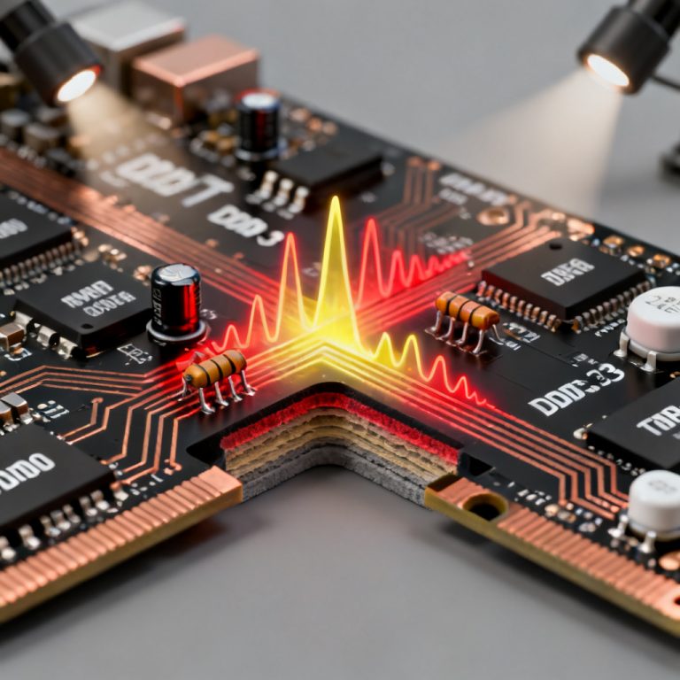
1. EMI – When Your PCB Becomes an Unintended Antenna
Electromagnetic Interference (EMI) has long been one of the biggest bottlenecks blocking electronic products from passing global EMC compliance certifications. As detailed in the High-speed PCB troubleshooting master page, pcb emi issues are among the most common signal integrity failures. For PCB designers and hardware engineers, EMI rarely happens by accident; it originates from flawed layout decisions, discontinuous signal return paths, high-speed clock harmonics, and uncontrolled common-mode current.
A widespread misconception is that EMI issues can be easily solved later by adding ferrite beads or metal shielding enclosures. In reality, these post-production remedies only suppress noise slightly and cannot eliminate fundamental design defects. The core principle every engineer must understand is simple: any poorly routed high-speed PCB will turn itself and connected cables into an unintended antenna. Effective EMI control must start at the PCB design phase. For Return Path design, maintaining continuous ground planes is the first line of defense against EMI.
2. Common Symptoms of PCB EMI Problems & Failure Stages
PCB emi issues do not always show up in the same way. They appear clearly in pre-lab testing, official EMC certification, or daily system operation. Recognizing these typical symptoms helps you judge the problem type early and avoid blind debugging.
| Symptom | Performance Manifestation | Failure Stage |
|---|---|---|
| Radiated Emissions Exceedance | Unwanted radio frequency signals radiate into the air, causing failure in open-field radiated emission certification tests | Formal EMC certification |
| Conducted Emissions Exceedance | Noise couples directly onto DC power lines, AC input lines, and external signal cables | Formal EMC certification |
| System Immunity & Functional Instability | Random rebooting, data loss, communication dropout, and unstable sensor readings | Functional verification |
| Narrowband Harmonic Spikes | Obvious fixed-frequency peaks appear, usually integer harmonics of main clocks | Pre-compliance testing |
By matching symptoms with testing stages, engineers can quickly distinguish whether the problem comes from radiated noise, conducted interference, or system-level immunity defects. For related troubleshooting, see PCB impedance issues and PCB crosstalk issues.
3. Root Causes of PCB EMI & Radiation Mechanisms
Nearly all pcb emi issues can be traced to five fundamental design causes, each corresponding to a clear radiation mechanism.
3.1 Excessive Current Loop Area & Broken Return Paths
High-speed signals always flow forward on the signal trace and return through the nearest ground plane. If the return path is cut off, routed too far, or blocked by plane splits, the current will form a much larger loop. Large loops generate strong differential-mode radiation, a major source of radiated EMI.
3.2 Uncontrolled Common-Mode Current
Asymmetric routing, unbalanced differential pairs, and long external cables easily induce common-mode noise. Even a tiny common-mode current on a cable can turn the cable into a highly efficient long antenna. Common-mode radiation is often far stronger than differential-mode noise.
3.3 Split Ground & Power Reference Planes
When high-speed traces cross split ground or power planes, the return path is forced to detour. This significantly enlarges the effective loop area, increases ground impedance, and aggravates both radiated and conducted emissions.
3.4 Fast Edge Rates & Clock Harmonics
High-speed clocks, DDR signals, and switching power waveforms with ultra-fast rise and fall edges contain rich high-order harmonics. These harmonics fall directly into the restricted frequency range of EMC standards, creating sharp narrowband spectrum spikes.
3.5 Disordered Grounding Strategy
Scattered multi-point grounding, isolated ground islands, and insufficient ground stitching vias create large ground loops and ground bounce noise. For PCB Manufacturing, proper grounding and plane design are essential for EMI control.
4. Locating EMI Sources with Near-Field Probes & Spectrum Analysis
Before modifying layouts or adding components, you must accurately find the exact EMI hotspot and corresponding frequency. Near-field probing is the most efficient, low-cost pre-compliance method.
| Tool | Core Purpose | Practical Operation |
|---|---|---|
| H-Field Probe | Locate high-frequency current sources; find loop radiation hotspots | Scan 2–5mm above PCB surface on high-speed traces, DC-DC converters, and connectors |
| E-Field Probe | Locate high-voltage noise radiation, plane resonance, edge leakage | Scan PCB edges, shield gaps, and unused plane areas |
| Spectrum Analyzer | Analyze frequency domain; match noise peaks with clock harmonics | Sync probe signals to analyzer, record dominant emission frequencies |
The standard process is: coarse scanning with a large probe → precise positioning with a small probe → spectrum frequency correlation → confirm the noise source before making any fixes. For PCB reflection issues, similar TDR-based localization techniques apply.
5. Proven Solutions to Reduce and Fix PCB EMI Issues
Solving pcb emi issues follows a layered strategy: PCB layout optimization, grounding improvement, passive component filtering, clock optimization, and metal shielding.
| Mitigation Measure | Targeted EMI Problem | Suppression Effect |
|---|---|---|
| Solid Unbroken Ground Plane | Excessive loop area, discontinuous return paths | High |
| Perimeter Ground Stitching Via Array | PCB edge radiation, plane resonance | High |
| Common-Mode Choke | Common-mode current on cables | Very High |
| Spread Spectrum Clocking | Narrowband harmonic spikes | High |
| π-Type Power Filter | Conducted emissions on power lines | High |
| Metal Shielding Can | Local high-noise component isolation | Very High |
A complete solid ground plane is the foundation of EMI control. Edge stitching vias suppress fringe electromagnetic field leakage. Common-mode chokes are the go-to solution for cable radiation. For High-Speed PCB Material, proper selection also impacts EMI performance.
6. Step-by-Step PCB EMI Troubleshooting Workflow
Follow this standardized 5-step workflow to troubleshoot pcb emi issues logically:
Step 1: Identify Over-Limit Frequencies – Use spectrum pre-testing to record all exceeding frequency points, separate narrowband clock harmonics from broadband switching noise.
Step 2: Locate Physical EMI Hotspots – Use E-field and H-field near-field probes to scan the board surface, pinpoint noise sources on specific components, traces, or cable connectors.
Step 3: Analyze Noise Coupling Paths – Determine whether the failure comes from differential-mode loop radiation, common-mode cable coupling, split reference planes, or power line conducted interference.
Step 4: Apply Targeted EMI Suppression Measures – Select layout optimization, grounding stitching, filtering components, or metal shielding according to root cause.
Step 5: Modify, Verify and Iterate – Re-scan with near-field probes after optimization, complete pre-compliance testing, and confirm emissions are within limits.
7. Pre-Compliance Testing Tips to Avoid Certification Failure
Formal EMC certification is expensive and time-consuming. Proper pre-compliance testing can greatly reduce failure risks when dealing with pcb emi issues.
First, always perform near-field hotspot scanning before official testing to fix obvious layout defects such as incomplete return paths and missing stitching vias in advance.
Second, correlate all spectrum noise peaks with system clock frequencies. Most narrowband over-limit points are direct harmonics of main oscillators and switching circuits.
Third, finish all layout adjustments, component additions, and shielding optimization during pre-testing. Never submit a product for full certification without pre-verification.
Finally, save spectrum comparison data before and after optimization to build an internal EMI design database for future projects.
8. Key Takeaways for EMI-Ready PCB Design
- PCB emi issues stem from poor PCB layout and grounding design, not component quality problems
- The core root causes are discontinuous return paths, excessive loop areas, common-mode current, split reference planes, and fast clock edge harmonics
- Complete ground planes, edge stitching vias, and controlled high-speed routing are the most cost-effective EMI prevention methods
- Near-field probing plus spectrum analysis is the fastest way to locate EMI hotspots without entering an anechoic chamber
- Follow the standardized 5-step troubleshooting flow and complete pre-compliance testing to greatly improve one-pass EMC certification success rate
For a complete understanding of all troubleshooting topics, return to the High-speed PCB troubleshooting master page.
9. FAQ About PCB EMI Issues & EMC Compliance
Q1: What is the main cause of PCB EMI failure?
Broken signal return paths, large current loops, common-mode noise on cables, split ground planes, and unmanaged clock harmonics are the top five causes.
Q2: Can I fix PCB EMI just by adding a metal shield?
Shielding only suppresses surface radiation; it cannot fix inherent loop and return path defects. Layout optimization is still essential.
Q3: Is near-field probing necessary for EMI troubleshooting?
Yes. It quickly locates hotspots without costly formal testing and is a standard tool for professional EMI debugging.
Q4: How to reduce clock harmonic EMI spikes?
Use spread spectrum clocking, slow down edge rates, add matching resistors, and keep clock traces short with complete ground reference.
Q5: Why do long external cables easily cause EMI failure?
Long cables act as efficient antennas for common-mode current; adding common-mode chokes is the most reliable fix.
10. Get Professional Help to Pass EMI/EMC Testing
Still struggling with persistent pcb emi issues, repeated EMC certification failures, high-speed layout optimization, or pre-compliance testing arrangement?
Our professional engineering team provides one-stop services including PCB EMI root cause analysis, layout EMC review, EMI troubleshooting solution design, and full-process guidance to help your products pass FCC, IEC, CE and global EMC compliance smoothly.
Whether you need technical consultation, layout revision guidance, customized EMI suppression solution design, or project quotation support, feel free to contact our team anytime. We will provide you with professional, industry-recognized practical solutions tailored to your PCB and product application scenarios.