Article Summary
Most hardware engineers and global procurement buyers hold a common misunderstanding: cutting high speed pcb cost saving must come at the expense of signal integrity, impedance control, thermal stability and product reliability. In fact, high speed pcb cost saving and stable high-speed performance are completely compatible. By making scientific decisions in PCB design stackup, material specification selection, manufacturing process optimization, DFM compliance, panel layout and bulk procurement planning, manufacturers and design teams can save 20% to 50% of overall high speed pcb cost saving budget without downgrading electrical performance or service life. This comprehensive high speed pcb cost saving guide integrates industry top manufacturer experience, professional PCB media best practices and mass production data, covering actionable strategies for prototype, small batch and mass production scenarios.
1. Smart Cost Reduction for High-Speed PCBs
Cutting high speed pcb cost saving does not mean sacrificing quality or performance. The biggest waste in high-speed PCB projects usually comes from over-engineering, over-specification, redundant layer design, blindly choosing ultra-high-end imported materials, overly strict process tolerances and scattered small-batch orders. As detailed in the high-speed PCB cost master page, understanding where costs come from is the first step to reducing them.
More than 60% of PCB manufacturing costs are locked in the early design stage. Reasonable layout stackup, standardized parameter setting and forward-looking DFM review can fundamentally avoid unnecessary expenses. With systematic optimization across design, materials, manufacturing, testing and procurement dimensions, most projects can achieve 20-40% regular high speed pcb cost saving, and over-engineered projects can even reach 50% savings.
This high speed pcb cost saving guide is tailored for professional hardware design engineers, purchasing managers and global industrial buyers. All tips are based on IPC industry standards and mass production practice, applicable from prototype verification to long-term mass production. Adopting these strategies can not only reduce budget expenditure, but also improve production yield, shorten lead time and lower after-sales hidden costs.
2. Design-Level High-Speed PCB Cost Savings
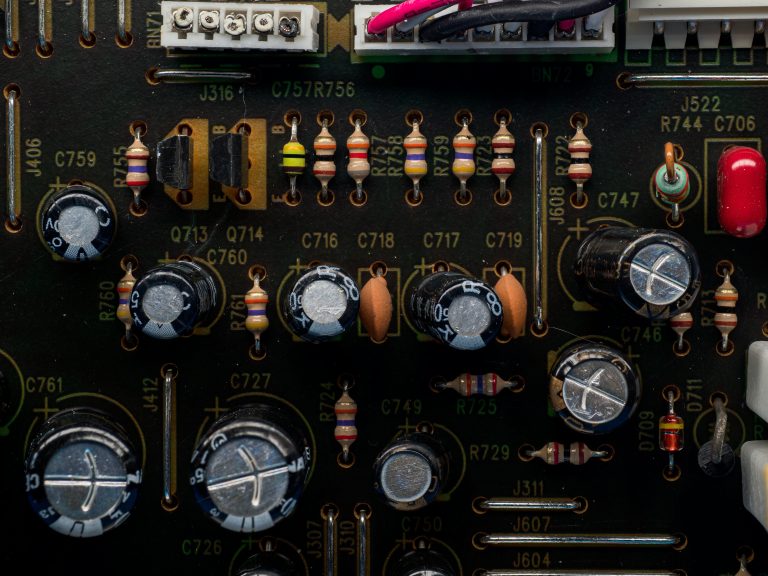
Design optimization is the highest return link for high speed pcb cost saving. Minor adjustments to stackup, line width/spacing, back-drilling and board specification can bring obvious cost reduction without damaging high-speed signal transmission quality. For pcb cost factors, design decisions have the greatest impact.
| Tactic | Saving Range | How It Works |
|---|---|---|
| Reduce redundant layer count | 20–50% | Merge redundant ground/power planes, reorganize routing layers |
| Adopt standard board thickness | 5–10% | Use 1.6mm standard; avoid custom non-standard thickness |
| Relax over-tight line width/spacing | 10–20% | Use 4/4mil instead of 3/3mil ultra-fine lines |
| Minimize unnecessary back-drilling | 5–15% | Apply back-drilling only on critical high-speed layers |
| Combine small designs for joint panel | 15–30% | Merge multiple designs to share engineering fees |
Layer count is the decisive factor of high speed pcb cost saving. Each additional layer increases lamination, drilling, substrate and testing costs exponentially. Designers can merge redundant ground and power planes, reorganize routing layers and optimize impedance stackup structure to remove 1-2 unnecessary layers while keeping signal integrity unchanged.
3. Material Selection & Hybrid Stackup Cost Optimization
Blindly selecting top-tier imported high-speed materials is one of the largest hidden cost wastes. The correct material selection logic for high speed pcb cost saving is matching material performance with actual application speed, rather than pursuing the highest specification uniformly. For detailed material data, see High-Speed PCB Material.
| Tactic | Saving Range | How It Works |
|---|---|---|
| Avoid over-specifying high-speed laminates | 20–50% | Deploy ultra-low-loss materials only for >16Gbps channels |
| Adopt hybrid lamination stackup | 10–25% | Combine FR4 for inner layers, high-speed material for outer layers |
| Certified domestic material substitution | 20–40% | Replace imported brands with qualified domestic equivalents |
| Bulk unified stocking & long-term agreement | 5–15% | Centralize purchasing, lock stable pricing |
High-Speed Material Classification Reference for Cost Saving:
- Standard FR4: Below 5Gbps, lowest cost for ordinary industrial control
- Mid-loss laminate: 5–16Gbps, cost-effective for WiFi 6/7 and consumer products
- Low-loss laminate: 16–56Gbps, for data center and network switch channels
- Ultra-low-loss RF material: Above 56Gbps, only for aerospace and high-end RF
Hybrid stackup is a powerful high speed pcb cost saving technique. Arrange expensive low-loss substrates only on top/bottom critical high-speed layers, and use ordinary FR4 for middle ground, power and non-critical inner layers. This method maintains impedance stability while cutting overall high speed pcb cost saving by 10-25%.
4. Manufacturing Process & Panelization Cost Saving
Even with fixed design and materials, unreasonable manufacturing process requirements will lead to extra cost. Optimizing panel layout, surface treatment, tolerance standard and testing mode can reduce comprehensive high speed pcb cost saving steadily. For PCB Manufacturing, process optimization is essential.
| Tactic | Saving Range | How It Works |
|---|---|---|
| Optimize panel layout for material utilization | 5–20% | Regular rectangular design, standardized multi-up panelization |
| Choose standard cost-effective surface finish | 5–15% | Use OSP or HASL instead of ENIG when possible |
| Relax unnecessary strict tolerance | 10–30% | Use ±15% instead of ±10% for non-critical dimensions |
| Optimize electrical testing mode | 5–10% | Batch sampling for mature designs instead of 100% testing |
A key high speed pcb cost saving insight: ultra-tight ±10% default tolerance increases manufacturing difficulty and rework rate. Relaxing non-critical position tolerance to industry standard ±15% matches mainstream factory process capability, reduces scrap and lowers overall cost. For mature mass-production high-speed PCBs with stable DFM design, adopt batch sampling inspection instead of 100% flying probe testing.
5. Volume Procurement & Order Planning Strategies
Scattered small orders, rush expedited production and fragmented supplier cooperation are important reasons for high comprehensive cost. Scientific order planning and procurement management can stabilize high speed pcb cost saving and shorten lead time. For high speed PCB mass production cost, volume discounts are significant.
| Tactic | Saving Range | How It Works |
|---|---|---|
| Merge scattered small orders into bulk | 15–25% | Eliminate repeated engineering and setup fees |
| Sign long-term fixed-quantity agreement | 10–20% | Lock stable pricing, priority production scheduling |
| Arrange production in standard schedule | 5–10% | Avoid urgent quick-turn rush order surcharges |
Merging multiple separate prototype replenishment orders into one bulk order is a powerful high speed pcb cost saving method. Repeated orders generate repeated engineering fees. Consolidation eliminates minimum order surcharges and reduces unit price significantly.
6. DFM-Driven Hidden Cost Reduction
DFM (Design for Manufacturability) is the hidden core of high speed pcb cost saving. Many invisible costs come from non-manufacturable design details, leading to repeated communication, file modification, high scrap rate and delayed delivery. For high speed PCB prototype cost, DFM issues are especially costly in small runs.
- Avoid unrealistic over-specification: Unreachable process parameters cause production bottlenecks and high rework loss. Set specifications strictly within mainstream PCB manufacturing capability.
- Complete and standardized design documents: Complete Gerber, stackup file, material specification and process requirement notes reduce repeated technical communication and file revision cost.
- Adopt standard unified via sizes: Custom special via sizes need customized drill bits, increasing tool loss and process difficulty. Using industry standard via dimensions can lower production cost and improve processing efficiency.
7. Combined Cost Savings Estimate & Practical Cases
A single optimization measure can bring stable partial savings, while superimposing multi-dimensional strategies of design, material, process, DFM and procurement can achieve total comprehensive high speed pcb cost saving of 25–50%.
The cost reduction effect is most obvious when projects transition from prototype small batch to formal mass production. For conventional network, communication and industrial high-speed PCBs, optimizing layer count + hybrid stackup material + panelization + DFM compliance can easily save 25–35%. For over-engineered projects with excessive layers and full-board imported high-end materials, comprehensive high speed pcb cost saving can reach 40–50% reduction, with no negative impact on signal integrity, thermal performance and long-term reliability.
Real industry case: A 16-layer network switch high-speed PCB adopted layer reduction + hybrid FR4 high-speed material + selective back-drilling + relaxed non-critical tolerance. The final total cost was reduced by 27%, while electrical performance and product service life remained completely unchanged – a perfect example of effective high speed pcb cost saving.
8. Key Takeaways
- High speed pcb cost saving is a full-lifecycle systematic project covering design, material selection, manufacturing process, DFM and procurement
- Layer count optimization and material grade selection are the two largest cost drivers with the highest saving potential
- Cost control must be planned in the early design stage, not remedied after production
- Standardization is the core of high speed pcb cost saving: standard board thickness, standard layers, standard surface treatment, standard via size and standard tolerance
- Merging orders and long-term procurement agreements are the most direct ways for purchasing teams to reduce comprehensive cost and stabilize lead time
9. FAQ About High-Speed PCB Cost Saving
Q1: Will relaxing line width and tolerance affect high-speed signal performance?
No. As long as the adjustment is within the impedance design calculation range and IPC standard, properly relaxing non-critical line width, line spacing and tolerance will not damage signal integrity, but can improve production yield and reduce high speed pcb cost saving targets.
Q2: Is domestic high-speed material reliable enough for industrial and network equipment?
Yes. Qualified certified domestic high-speed laminates have passed UL, RoHS and long-term thermal cycling tests, with Dk/Df parameters matching imported brands. This is a proven high speed pcb cost saving method.
Q3: What is the fastest way to cut high-speed PCB cost without modifying design?
Optimize panel utilization, switch to standard surface finish, merge small orders and adopt sampling testing mode. These measures need no design change and can save 5–20% cost quickly.
Q4: How much cost can hybrid stackup save in general?
Reasonable hybrid lamination combining FR4 and high-speed materials can save 10–25% of material cost on average, suitable for multi-layer high-speed PCB above 8 layers.
Q5: Can I achieve both cost saving and high performance?
Absolutely. The entire premise of this high speed pcb cost saving guide is that cost optimization and performance are compatible when done correctly through intelligent design and material choices. For more on the trade-offs, refer to high speed PCB mass production cost and high speed PCB prototype cost.
10. Get Cost-Optimized PCB Quote & Design Review
Want to optimize your existing high-speed PCB design for high speed pcb cost saving, or get a customized budget-friendly quotation for new projects?
Our professional technical team provides one-stop services: PCB stackup optimization, DFM design review, high-speed material alternative recommendation, process parameter tuning and panelization scheme design. We help you save 20-50% PCB cost while fully maintaining high-speed signal performance and product reliability.
Submit your PCB design files and project requirements now, and get a free professional cost optimization analysis and competitive wholesale quote within the shortest time.