The complete High Speed PCB Design workflow from schematic to fabrication is a structured, iterative process that ensures signal integrity, power integrity, and manufacturability. This guide covers every critical step for reliable High Speed PCB performance.
High Speed PCB Design Pre-Layout Planning
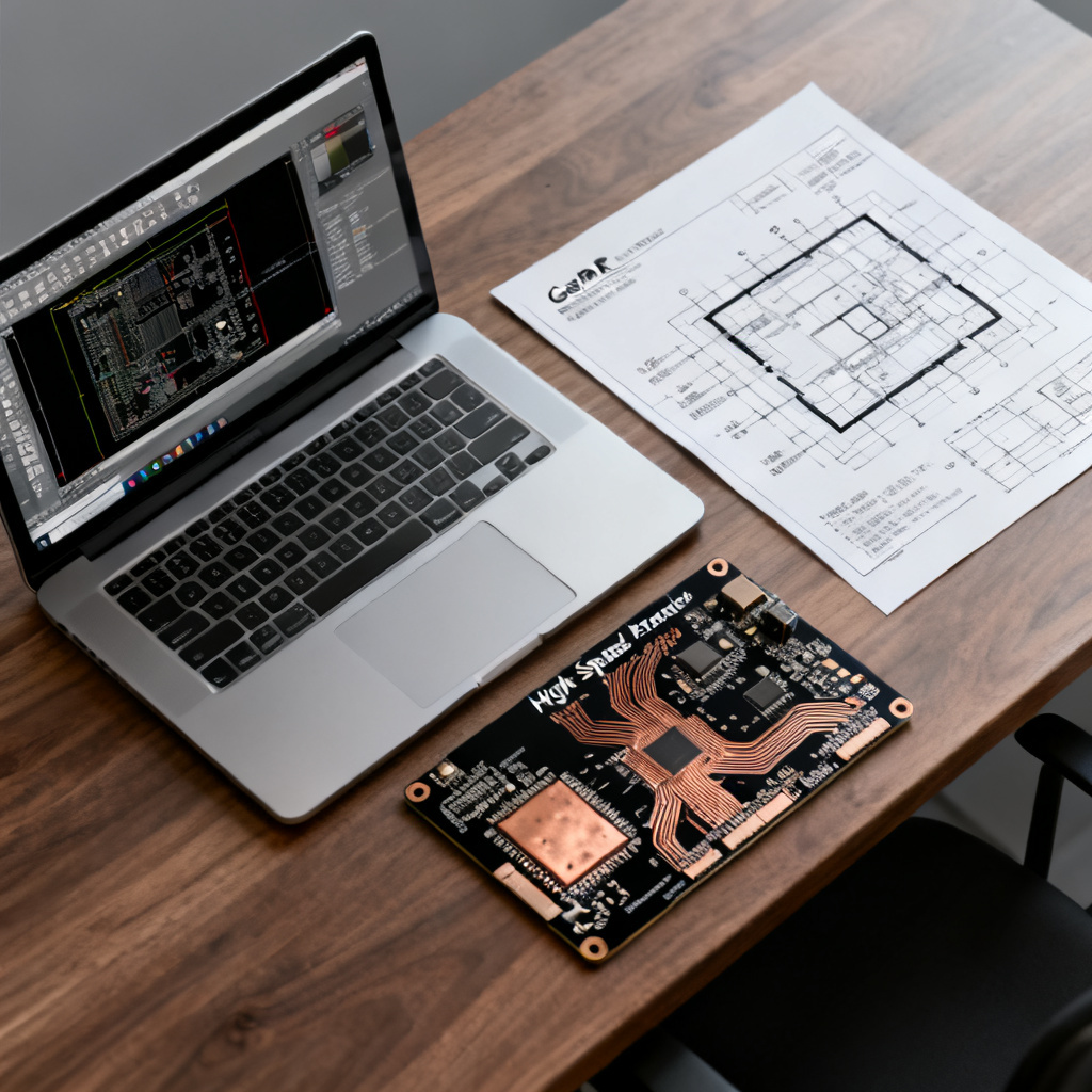
The foundation of any successful High Speed PCB Design is a meticulously crafted schematic and a well-defined pre-layout strategy. This phase is where electrical requirements meet physical constraints, ensuring a smooth transition into layout.
Component Selection & Stack-Up Planning
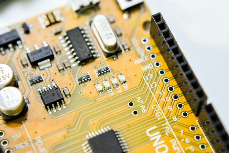
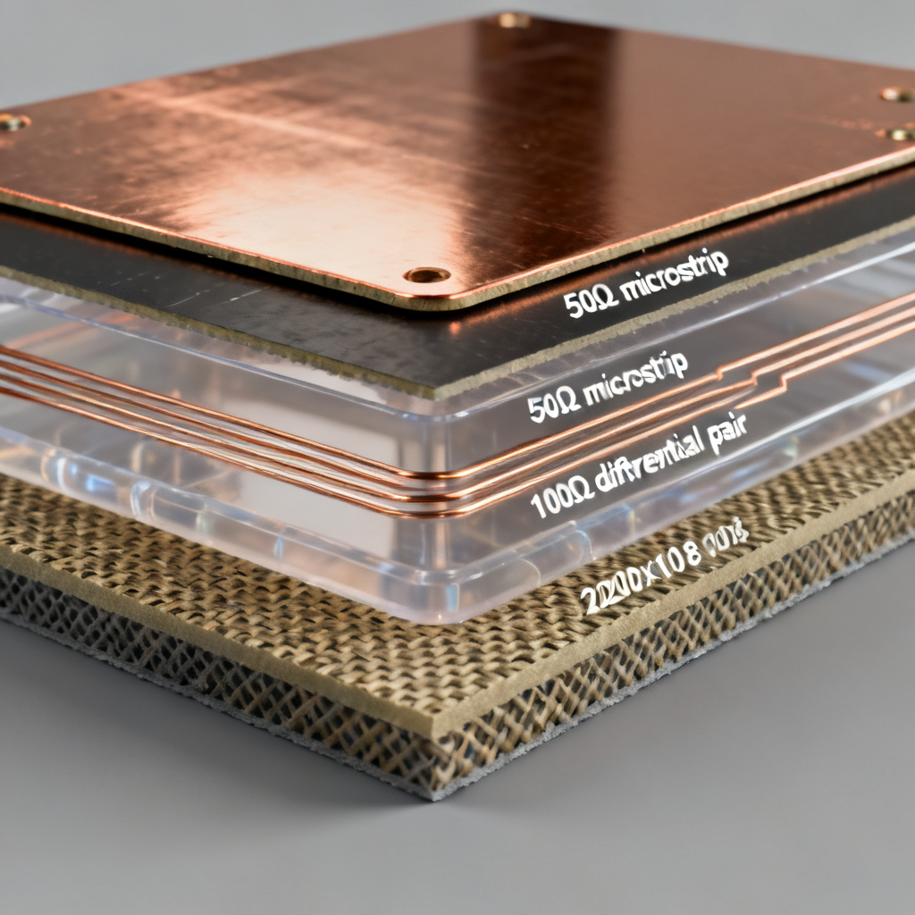
Before placing a single symbol, the designer must select components that meet the target data rates. Key considerations include signal integrity models (IBIS or IBIS-AMI), power integrity requirements, and stack-up definition. The PCB stack-up is the single most important factor in controlling impedance and crosstalk. A typical High Speed stack-up might include signal layers (stripline and microstrip), solid reference planes (GND, VCC), and low-loss dielectric materials like Rogers, Isola, or Panasonic for high-frequency applications above 1 GHz.
Altium emphasizes that the stack-up must be defined before layout to calculate target impedance, such as 50Ω single-ended or 100Ω differential. A minimum of 4 layers is recommended for High Speed; 8-16 layers are common for complex digital systems.
Schematic Capture & Net Grouping
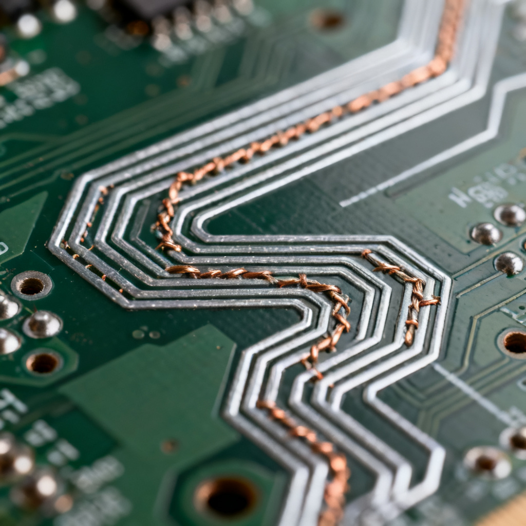
The schematic must be more than a connectivity diagram. It must be a data-rich document with explicit net labels (e.g., PCIe_TX_P, DDR_DQ[0:31]), class creation for nets (e.g., HIGH_SPEED, CLOCK, POWER), and clear definition of differential pairs. Most EDA tools allow you to pair nets and assign a target impedance.
Sierra Circuits recommends creating a Design for Manufacturing (DFM) checklist at this stage, noting any special fabrication requirements like controlled impedance testing or via filling.
Pre-Layout Simulation & Constraint Definition
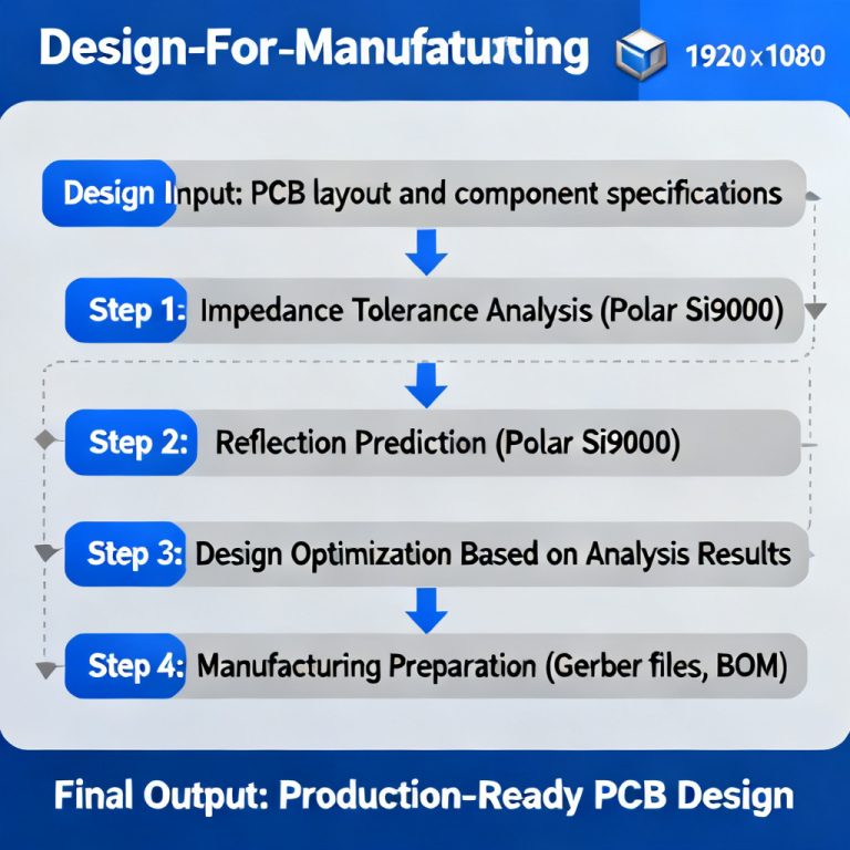
This step is often overlooked but is crucial for High Speed success. Before a single trace is routed, perform signal integrity pre-layout analysis using tools like HyperLynx or Sigrity to validate topology, termination, and length limits. Then, populate the Constraint Manager with impedance rules (50Ω ±10% single-ended, 100Ω ±10% differential), length matching tolerances, spacing rules (3W rule), and via restrictions.
Cadence highlights that the Constraint Manager is a living document that drives the autorouter and real-time DRC during layout.
High Speed PCB Layout & Routing
This is the most time-intensive phase, where the theoretical design becomes physical reality. For High Speed signals, every millimeter and every via matters.
Component Placement: The Art of Signal Flow
Component placement is not about packing parts; it is about optimizing signal paths. Place High Speed components (FPGA, transceivers, memory) near their connectors. Keep analog, digital, and power sections physically separated. Place decoupling capacitors as close as possible to the power pins of ICs, minimizing loop area. Route High Speed signals directly from the IC to the connector without unnecessary detours.
Routing High-Speed Nets: Rules of the Road
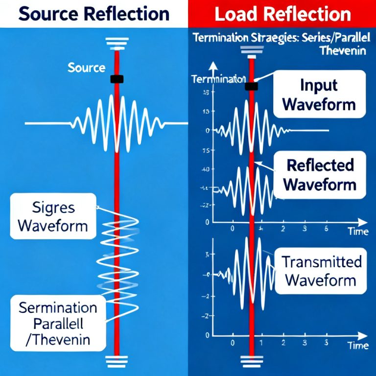
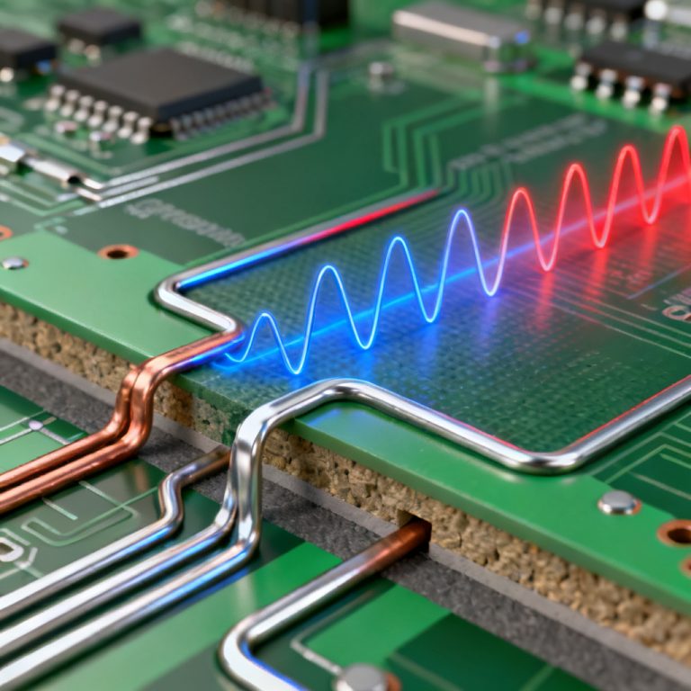
Routing is where the constraints from pre-layout are enforced. Adhere to trace geometry rules (width calculated from stack-up, spacing per 3W rule), use 45-degree corners exclusively, and manage layer transitions (vias) carefully. For vias, avoid long via stubs by using back-drilling or blind/buried vias for signals above 5 GHz. Ensure a ground via is within 1 mm of the signal via to provide a continuous return path.
Power Delivery Network (PDN) Design
A clean PDN is as critical as signal routing. Use solid copper pours for power rails, avoid splitting planes, and implement a decoupling strategy with bulk, mid-frequency, and high-frequency capacitors. Target a PDN impedance below 10 mΩ for 1.0V rails across the frequency range of interest (DC to 1 GHz).
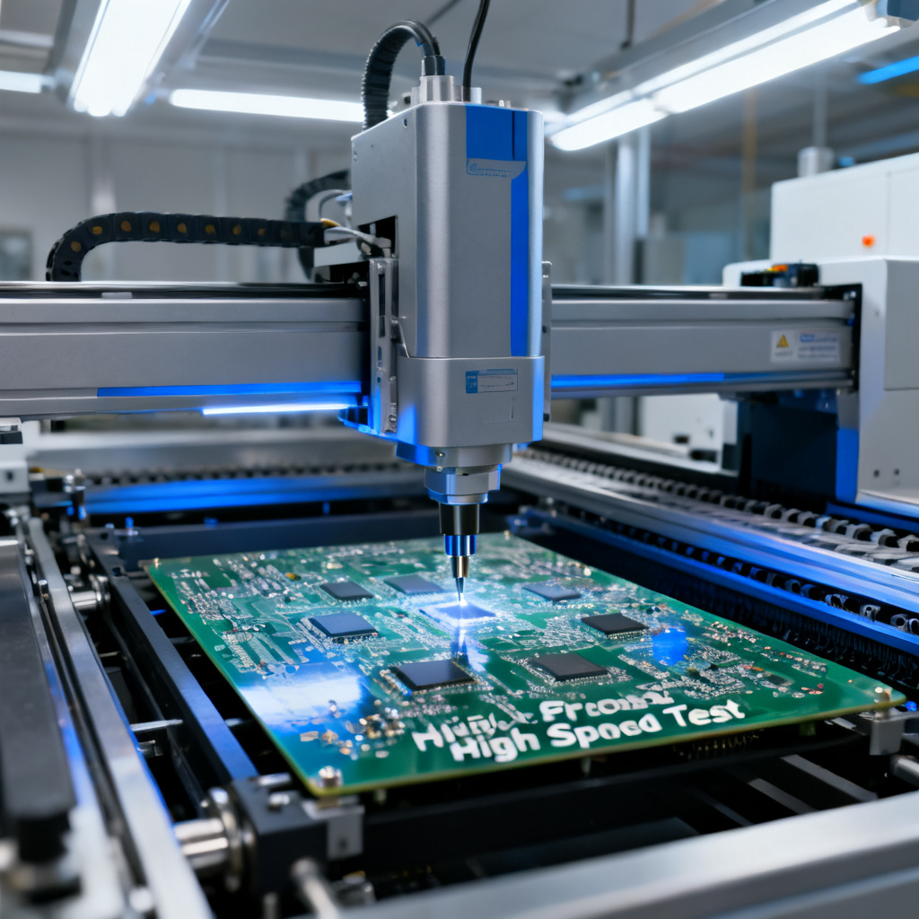
High Speed PCB Verification & Simulation
After routing, the design must be validated before fabrication. This phase catches errors that DRC cannot.
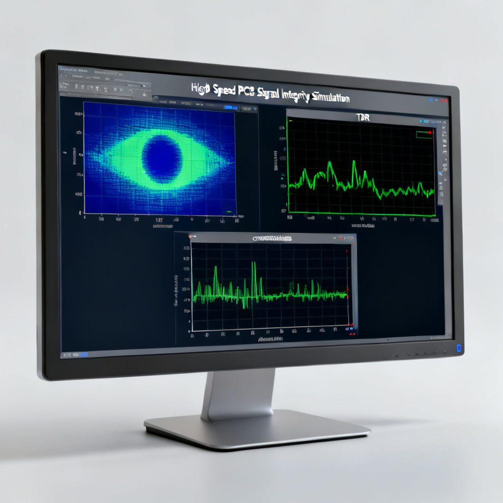
Signal Integrity (SI) Simulation
Use extracted parasitics from the layout to run time-domain simulations. Generate eye diagrams for differential pairs (e.g., PCIe, USB 3.0), simulate TDR to identify impedance discontinuities, and analyze crosstalk (NEXT and FEXT) on adjacent traces.
Power Integrity (PI) Simulation
Simulate DC voltage drop (IR drop) across the plane to ensure all ICs receive the minimum required voltage. Use frequency-domain simulation to verify that the PDN impedance is below the target across the bandwidth.
Design Rule Check (DRC) & Manufacturing Checks
Re-run the electrical DRC to ensure all constraints are met. Perform DFM checks for minimum annular ring, clearance between copper and board edge, solder mask slivers, and minimum trace width/spacing for the fabricator.
High Speed PCB Fabrication & Assembly
The final phase translates the digital design into a physical product. This is where the relationship between designer and manufacturer becomes critical.
Generating Fabrication Files (Gerber & ODB++)
The standard output is a set of Gerber RS-274X files or ODB++ for data richness. Include all copper layers, solder mask layers, silkscreen layers, drill file (Excellon format), and a netlist. Provide a stack-up drawing showing layer order, material types, thickness, and target impedance values. Add a readme file with special instructions.
Key Fabrication Specifications for High Speed Boards
| Specification | High Speed PCB Requirement |
|---|---|
| Controlled Impedance | Test on coupons; tolerance ±10% (standard) or ±5% (premium) |
| Back-Drilling | For thick boards (>2mm) with High Speed signals to remove via stubs |
| Material Selection | High-frequency laminates (e.g., Rogers 4350B) with exact Dk tolerance |
| Surface Finish | ENIG preferred for High Speed; avoid HASL for fine-pitch BGA |
Assembly Considerations
Design the solder paste stencil based on component pitch. Consider panelization for assembly efficiency. Plan for flying probe or bed-of-nails testing, adding test points to critical High Speed nets if possible.
FAQ: High Speed PCB Design Workflow
What is the most critical step in the High Speed PCB Design workflow?
The most critical step is pre-layout planning, including stack-up definition and constraint setup, as it directly impacts signal integrity and power integrity throughout the High Speed PCB Design process.
How does the High Speed PCB Design workflow ensure manufacturability?
The workflow incorporates DFM checks, controlled impedance specifications, and clear fabrication file generation (Gerber/ODB++) to ensure the High Speed PCB Design is reliably produced by manufacturers.
What tools are recommended for High Speed PCB Design simulation?
Industry-standard tools include HyperLynx (Siemens) and Sigrity (Cadence) for signal integrity and power integrity simulation, which are integral to a professional High Speed PCB Design workflow.
“`