Laser drilling has become the most reliable microvia forming method for HDI miniaturized circuits and high-speed signal-controlled PCBs. As electronic products trend toward miniaturization and high-frequency performance upgrading, traditional mechanical drilling can no longer meet ultra-fine interconnection demands. Laser drilling hdi pcb adopts focused laser energy to ablate dielectric and copper foil in a non-contact way, delivering ultra-small aperture, high positional accuracy, and stable impedance performance ideal for high-speed PCB layout.
The PCB Manufacturing & Testing Guidelines provides a complete overview of all manufacturing processes, including laser drilling. This guide integrates global top laser equipment technology and actual PCB mass production experience, explaining laser classification, microvia parameters, complete manufacturing workflow, DFM guidelines and common production defects. Understanding laser drilling hdi pcb is essential for modern HDI and high-speed board manufacturing.
Table of Contents
- 1. What Is Laser Drilling in HDI & High-Speed PCB Production
- 2. Working Principle of Laser Drilling for Microvia Fabrication
- 3. CO2 Laser vs UV Laser: Full Technical Comparison
- 4. Standard & Advanced Microvia Technical Parameters
- 5. Complete Laser Drilling Process Flow
- 6. Critical DFM Design Rules for Laser Microvias
- 7. Laser Drilling vs Mechanical Drilling Practical Comparison
- 8. Common Laser Drilling Defects, Causes and Solutions
- 9. Main Application Scenarios of Laser Drilling
- 10. Key Takeaways for Designers and Manufacturing Teams
- 11. FAQ About Laser Drilling for HDI and High-Speed PCB
- 12. Professional Engineering Support
What Is Laser Drilling in HDI & High-Speed PCB Production
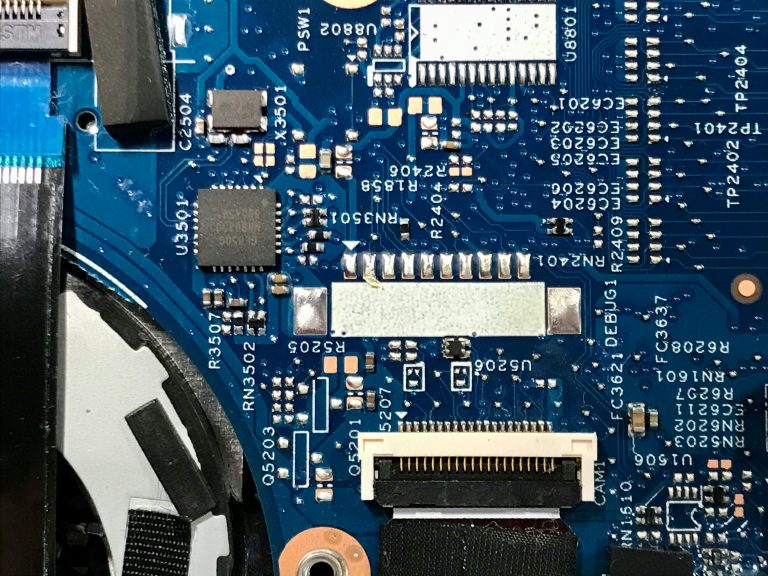
Laser drilling is a non-contact high-precision manufacturing process dedicated to forming blind microvias, stacked vias and ultra-fine interconnection holes in multilayer HDI and high-speed PCBs. Different from conventional mechanical drilling with rotating drill bits, it uses high-energy focused laser beams to vaporize and ablate resin, glass fiber and copper foil materials, stably producing microvias smaller than 0.1mm.
In high-speed PCB design, signal integrity and impedance stability are core indicators. Mechanical drilling easily brings substrate stress, board deformation and inner layer delamination, while laser drilling completely avoids physical extrusion and vibration. For high-density HDI layouts, laser drilling hdi pcb is the standard process adopted by mainstream factories worldwide, supporting first-order to third-order HDI boards and any-layer interconnection structure design.
For detailed HDI structure information that uses laser drilling, the HDI PCB Manufacturing Guide provides comprehensive coverage of stackup and layer arrangements for laser drilling hdi pcb applications.
Working Principle of Laser Drilling for Microvia Fabrication
The core working principle of laser drilling is precise thermal ablation and cold photon etching. The equipment relies on high-precision CCD visual alignment to position the PCB panel accurately, then emits pulsed laser beams to irradiate the preset microvia area.
Concentrated instantaneous laser energy removes dielectric materials layer by layer, accurately stopping at the target inner layer to form standard blind microvias. The whole process requires no physical contact with the board surface, so the substrate keeps flat without internal mechanical stress.
The formed microvia features smooth hole walls, stable dimensional tolerance and good adhesion for subsequent chemical copper deposition and electroplating, which is fundamental to guarantee high-speed signal transmission quality and long-term circuit reliability in laser drilling hdi pcb manufacturing.
CO2 Laser vs UV Laser: Full Technical Comparison
In commercial PCB mass production, CO2 laser and UV laser are the two mainstream laser drilling solutions. Their wavelength characteristics, material absorption capacity, processing limit and application positioning are significantly different, which directly determines the manufacturing grade and cost of HDI and high-speed PCB projects.
| Comparison Item | CO2 Laser | UV Laser |
|---|---|---|
| Wavelength | 9.4–10.6μm infrared | 355nm ultraviolet |
| Material Absorption | Excellent for dielectric and glass fiber, poor for copper | Absorbs both copper foil and dielectric evenly |
| Minimum Aperture | ≥0.1mm | 0.075–0.1mm |
| Hole Wall Quality | Good with slight resin residue | Outstanding, smooth wall, low heat-affected zone |
| Copper Processing | Needs pre-opening copper window | Direct drilling through copper without pre-process |
| Cost Level | Low operation and equipment cost | Higher investment and production cost |
| Main Application | Standard HDI mass production | High-speed PCB, high-end HDI, IC packaging substrate |
CO2 laser is cost-effective and stable in ablation for conventional dielectric materials, making it the preferred choice for cost-sensitive standard HDI projects. The Blind and Buried Vias Guide, which covers ultra-fine microvia applications in detail, provides additional design recommendations that complement laser drilling hdi pcb technology. UV laser adopts cold processing technology, with smaller thermal impact and ultra-fine drilling capability, perfectly matching the strict precision requirements of high-speed high-frequency boards and stacked via design.
Standard & Advanced Microvia Technical Parameters
Microvia parameter standards define the process capability boundary of laser drilling, and are the basic basis for PCB DFM design and production feasibility evaluation. All parameters comply with IPC industry norms, divided into standard industrial capability and advanced UV laser capability.
| Technical Parameter | Standard Capability | Advanced UV Laser Capability |
|---|---|---|
| Minimum Aperture | 0.1mm | 0.075mm |
| Maximum Drilling Depth | 4mil (≈0.1mm) | 6–8mil |
| Aspect Ratio | ≤1:1 | ≤1.2:1 |
| Hole Position Accuracy | ±1mil | ±0.5mil |
Aspect ratio, calculated by microvia depth divided by aperture diameter, is the most critical reliability index for laser drilling hdi pcb. For conventional design, controlling the aspect ratio within 1:1 can ensure complete desmear and hole metallization without internal voids. Advanced UV laser process can stably support 1.2:1 aspect ratio under precise parameter control, suitable for thicker high-speed substrate applications. Higher positioning accuracy also guarantees the alignment effect of stacked vias in high-density layout.
Complete Laser Drilling Process Flow
The standardized industrial laser drilling workflow ensures consistent microvia forming quality and follows a fixed sequential process:
Copper Window Opening → Laser Dielectric Ablation → Desmear Treatment → Microvia Metallization → Plug Hole Electroplating
Copper window opening is mainly for CO2 laser process, etching off surface copper foil to expose the dielectric layer for laser ablation; UV laser can omit this step and drill directly. The Back Drilling Process Guide, which covers an alternative hole formation technique for through-hole vias, can be used alongside laser drilling hdi pcb for different via requirements. After laser forming microvias, chemical or plasma desmear removes residual resin and burrs on hole walls to smooth the inner wall. Then chemical copper deposition and electroplating form a conductive copper layer to realize interlayer conduction. For stacked via structure, plug hole electroplating fills the microvia completely to enhance structural stability and avoid lamination cracking.
Critical DFM Design Rules for Laser Microvias
Reasonable design rules can avoid production bottlenecks, reduce revision costs and improve the yield of HDI and high-speed PCB.
| Design Rule | Specific Requirement |
|---|---|
| Pad Annular Ring | Aperture plus 0.2–0.25mm |
| Adjacent Microvia Spacing | ≥0.3mm |
| Stacked Via Process | Plug hole electroplating required before upper lamination |
| Layout Suggestion | Avoid continuous multi-layer stacked vias |
Sufficient pad annular ring can tolerate minor hole position deviation to prevent open circuit and pad falling off. Reasonable spacing between microvias avoids laser thermal interference and substrate delamination, and also suppresses crosstalk for high-speed signals. Stacked vias without full plug hole electroplating are prone to reliability risks in thermal cycling and reflow soldering. These DFM rules are critical for successful laser drilling hdi pcb production.
Laser Drilling vs Mechanical Drilling Practical Comparison
Mechanical drilling is still widely used in conventional PCB production, but it has obvious limitations in high-density and high-speed scenarios.
| Comparison Item | Laser Drilling | Mechanical Drilling |
|---|---|---|
| Minimum Aperture | 0.075mm | 0.2mm |
| Hole Wall Stress | No mechanical stress | Obvious mechanical impact stress |
| Precision | Ultra-high | Limited by drill bit precision |
| Unit Cost | Higher | Lower |
| Application Scope | Micro blind vias, HDI, high-speed PCB | Ordinary through-holes, low-density PCB |
Mechanical drilling is cost-effective for large-aperture through-holes, but cannot break the 0.2mm aperture limit. Laser drilling makes ultra-fine microvias possible, with no substrate deformation and better impedance consistency. Most industrial projects adopt a hybrid solution: mechanical drilling for through-holes and laser drilling hdi pcb for microvias to balance performance and cost.
Common Laser Drilling Defects, Causes and Solutions
In mass production, improper parameters, material differences or positioning deviation will cause typical quality defects.
| Defect | Cause | Solution |
|---|---|---|
| Hole not fully penetrated | Insufficient laser energy, focus deviation | Adjust laser power, calibrate focusing system |
| Rough hole wall | Uneven dielectric material, unreasonable ablation speed | Optimize layered ablation parameter, strengthen desmear |
| Hole position offset | CCD alignment drift, board positioning slip | Regularly calibrate visual system, fix fixture stability |
| Copper foil curling | Incomplete pre-window etching | Adopt UV laser direct drilling, optimize etching parameters |
Daily equipment maintenance and classified parameter setting for different substrates can effectively reduce defect rates, which is especially critical for high-speed PCB with strict signal performance requirements in laser drilling hdi pcb manufacturing.
Main Application Scenarios of Laser Drilling
Laser microvia technology is widely used in high-end manufacturing fields with high density and high signal integrity requirements:
- 1st to 3rd order HDI PCBs and any-layer interconnection boards
- 5G communication, RF microwave and high-speed high-frequency circuit boards
- Automotive electronics, medical devices and aerospace precision PCBs
- Wearable equipment, smart consumer electronics motherboards
- IC packaging substrates and ultra-thin high-precision multilayer boards
Key Takeaways for Designers and Manufacturing Teams
- CO2 laser fits cost-controlled conventional HDI projects, while UV laser is more suitable for ultra-fine aperture and high-precision high-speed PCB design
- Keep microvia aspect ratio within 1:1 for universal reliability; stacked via design must match plug hole electroplating process for laser drilling hdi pcb
- Follow standard DFM rules for pad size and microvia spacing to avoid design risks
- The combination of laser drilling and mechanical drilling remains the most economical and efficient solution for most multilayer PCB projects
FAQ About Laser Drilling for HDI and High-Speed PCB
Q1: What is the smallest microvia size achievable by laser drilling?
Standard CO2 laser supports 0.1mm minimum aperture, while advanced UV laser can reach 0.075mm for laser drilling hdi pcb applications.
Q2: What is the safest aspect ratio for laser microvias?
1:1 is the industry universal safe standard; advanced process can reach 1.2:1 with manufacturer process confirmation.
Q3: Should I choose CO2 or UV laser for HDI PCB?
Choose CO2 for regular cost-sensitive HDI mass production; choose UV for smaller vias, stacked vias and high-speed high-frequency boards. This is a key decision in laser drilling hdi pcb planning.
Q4: Can laser drilling fully replace mechanical drilling?
Not completely. Mechanical drilling is still more cost-effective for conventional large through-holes; the two processes are usually used together.
Professional Engineering Support
If you are working on HDI layout, high-speed PCB design or stacked via structure planning, understanding laser drilling hdi pcb process capability and DFM rules in advance can effectively avoid design revisions and production delays.
We offer: HDI stackup design • Laser drilling process optimization • Microvia parameter evaluation • DFM review • Professional manufacturing quotation
Submit your project details for a professional technical review and competitive quote.
About HighSpeedPCBs.com
We are a specialized PCB design and manufacturing service provider serving industrial, automotive, medical, and communications OEMs worldwide. Our expertise in laser drilling hdi pcb ensures your high-density and high-speed designs are manufacturable and reliable. Complete manufacturing process documentation is available in the PCB Manufacturing & Testing Guidelines.
© 2026 HighSpeedPCBs.com — Professional High-Speed PCB Solutions