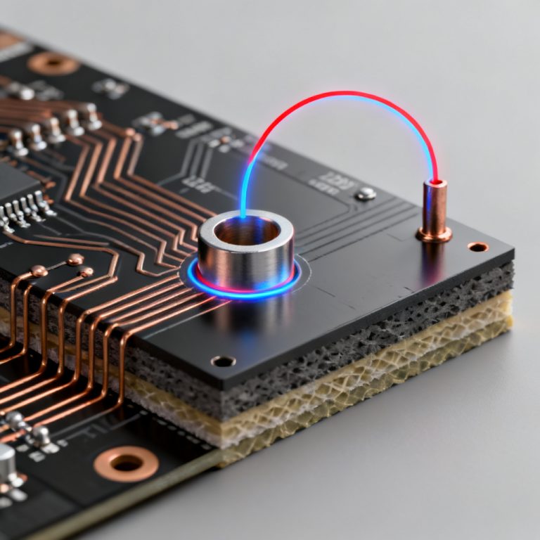
In high-speed PCB design, understanding how solder mask and surface finish affect impedance control PCB accuracy is critical for signal integrity. Even a perfectly calculated trace will fail if these two layers are ignored.
How Solder Mask Affects Impedance Control PCB Accuracy
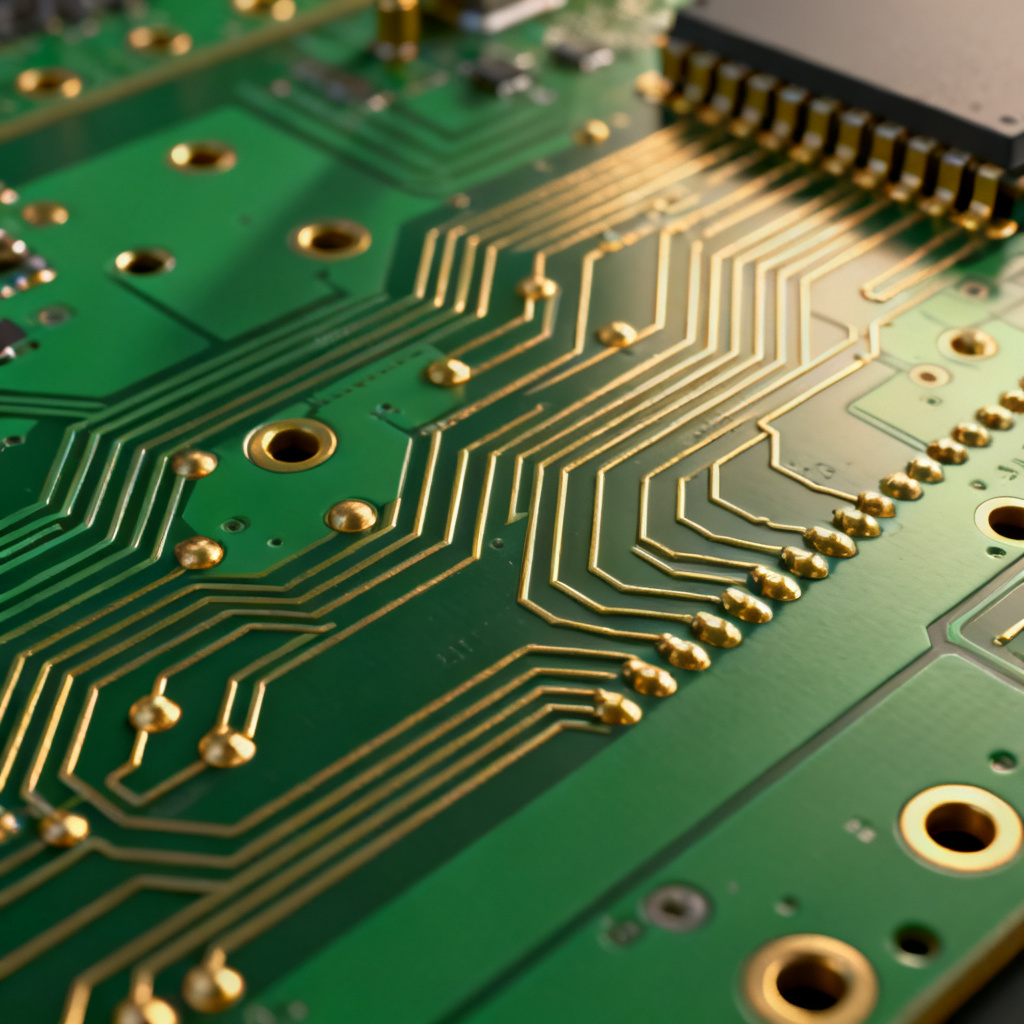
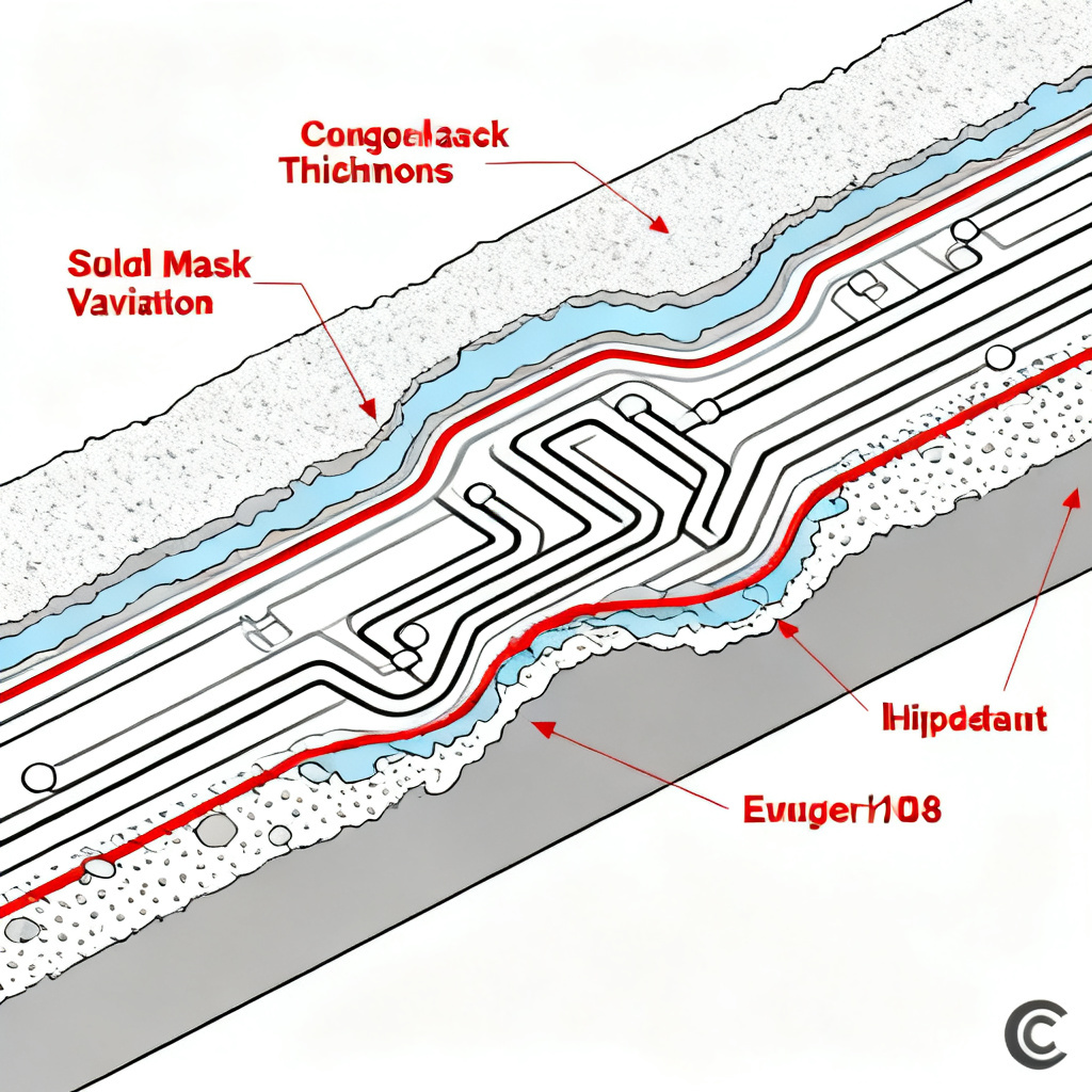
The solder mask is a dielectric layer that directly alters how solder mask and surface finish affect impedance control PCB accuracy on outer layers. Its dielectric constant (Dk) and thickness are the primary variables.
Solder Mask Dielectric Constant (Dk) Effect
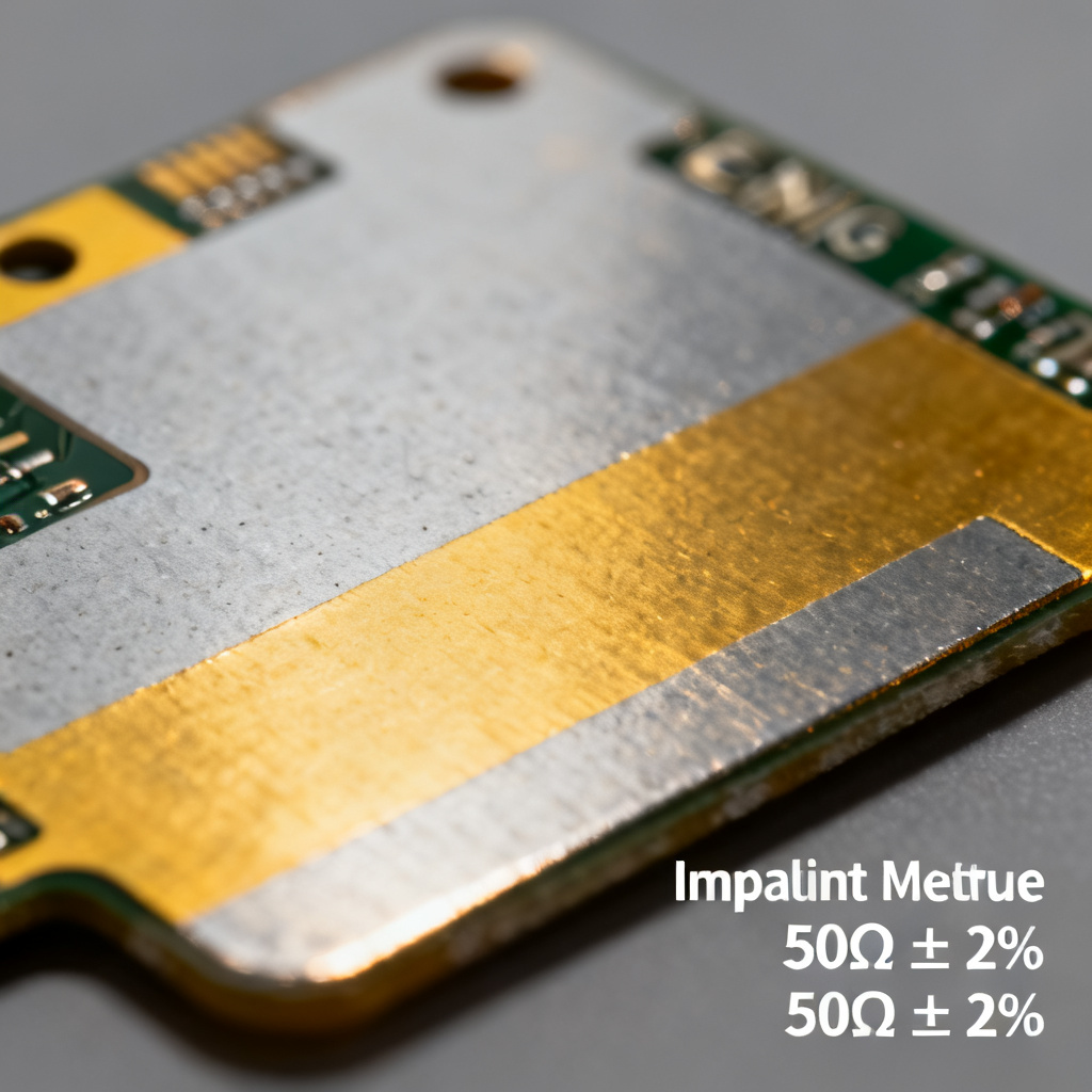
Solder mask typically has a Dk between 3.3 and 4.5, higher than air (Dk ≈ 1). When applied over a microstrip trace, the electric field lines pass through this higher-Dk material, increasing the effective dielectric constant and reducing characteristic impedance. A typical 0.5 mil layer can reduce impedance by 2 to 5 ohms on a 50-ohm trace. At frequencies above 1 GHz, this effect becomes more pronounced because the field is more concentrated near the trace surface.
Thickness Variability and Its Impact on Impedance Control PCB Accuracy
Solder mask thickness is non-uniform: thinner over trace tops (0.3–0.8 mils) and thicker in valleys (0.8–1.5 mils). This variation directly translates to impedance inconsistency. A change from 0.3 mil to 1.0 mil can cause a 3–8 ohm shift, which is a 6–16% error for a 50-ohm target—unacceptable for high-speed designs.
Solder Mask Color and Material Differences
Green solder mask has a Dk of 3.5–4.0, while black mask has a higher Dk (4.0–4.5) and higher loss tangent, leading to greater impedance reduction and signal attenuation. White mask may have a lower Dk (3.3–3.8) but is often thicker. LPI masks are common, but dry film masks offer tighter thickness control.
Accounting for Solder Mask in Impedance Calculations
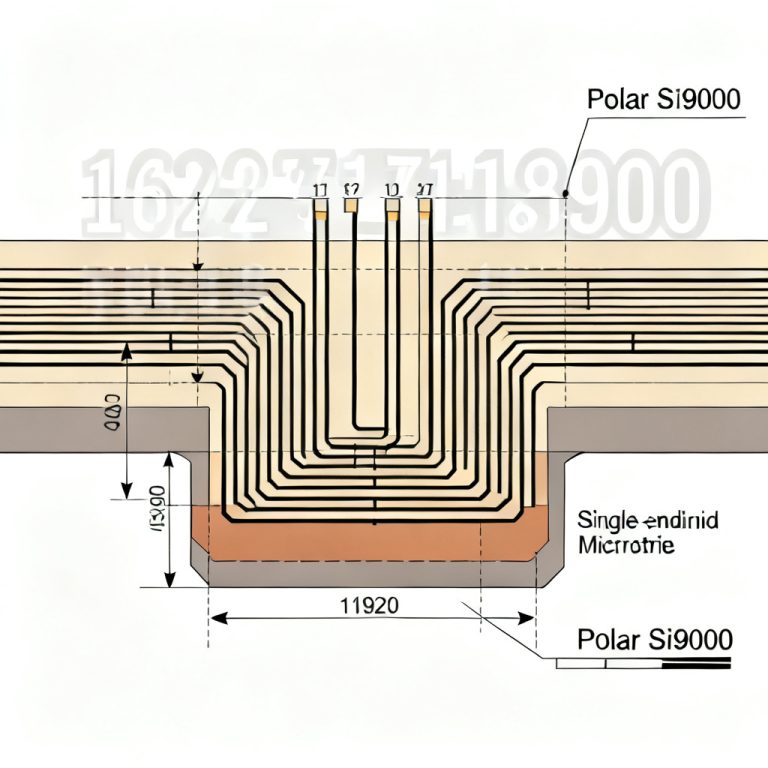
To maintain impedance control PCB accuracy, include solder mask in pre-layout impedance calculations using field solvers like Polar Si9000. Model the trace with a solder mask layer of 0.5–1.0 mil thickness and Dk 3.5. You may need to increase trace width by 0.5–2 mils to compensate. Always request impedance coupons with and without solder mask from your fabricator.
How Surface Finish Affects Impedance Control PCB Accuracy
The surface finish adds a conductive layer that influences how solder mask and surface finish affect impedance control PCB accuracy. At high frequencies, the current flows primarily in the surface finish layer due to skin effect.
The Conductive Layer Effect
Surface finishes like ENIG, HASL, Immersion Silver, and Immersion Tin add a thin conductive metal over copper. At 1 GHz, skin depth in copper is approximately 2 µm. ENIG’s nickel layer (3–6 µm) has lower conductivity than copper (σ_Ni ≈ 22% of σ_Cu) and is ferromagnetic, increasing resistance and inductance. This leads to higher impedance and higher loss. Gold (0.05–0.1 µm) is negligible. HASL is non-uniform (10–25 µm), causing impedance variation.
Impedance Shift by Finish Type
| Surface Finish | Typical Thickness | Conductivity Relative to Cu | Impedance Shift (vs. bare Cu) | Key Concern |
|---|---|---|---|---|
| ENIG | Ni: 3–6 µm; Au: 0.05–0.1 µm | Ni: ~22% | +1 to +3 ohms (increase) | Higher loss; nickel magnetic effects |
| HASL (SnPb) | 10–25 µm | ~85–90% | -0.5 to +1 ohm (variable) | Thickness non-uniformity |
| Immersion Silver (ImAg) | 0.15–0.5 µm | ~95–100% | -0.2 to +0.5 ohm | Very thin; minimal effect |
| Immersion Tin (ImSn) | 0.8–1.2 µm | ~90–95% | -0.3 to +0.6 ohm | Thin; minimal effect |
| OSP (Organic Solderability Preservative) | 0.2–0.5 µm (organic) | Insulator | No effect | Ideal for impedance control |
| Hard Gold (ENEPIG) | Ni: 3–6 µm; Pd: 0.05–0.1 µm; Au: 0.05–0.1 µm | Similar to ENIG | +1 to +3 ohms | Additional palladium layer adds slight inductance |
For high-speed designs above 5 GHz, OSP is the preferred finish because it does not alter copper’s electrical properties. If ENIG is required, you must account for the +1 to +3 ohm impedance increase.
Surface Roughness and Its Interaction with Impedance Control PCB Accuracy
Surface finish application processes, especially ENIG’s nickel plating, can increase copper surface roughness. A 1–2 µm increase in RMS roughness can increase conductor loss by 10–20% at 10 GHz. This does not directly change characteristic impedance but increases attenuation. Use low-roughness copper foils and specify controlled plating processes.
Practical Recommendations for Surface Finish Selection
For impedance-critical designs below 5 GHz, OSP is the safest choice. If OSP is not feasible, use Immersion Silver or Immersion Tin. For designs above 5 GHz, avoid ENIG unless absolutely necessary. If ENIG is required, compensate by reducing trace width by 0.5–1 mil or increasing dielectric height by 5–10% in your impedance model. For mixed-signal boards, use selective finishes: ENIG for BGA pads and OSP or ImAg for high-speed traces. Always request impedance test data with the specific surface finish applied.
Combined Effect of Solder Mask and Surface Finish on Impedance Control PCB Accuracy
In real-world manufacturing, both layers are present on outer layers. Their effects are additive but not always linear.
The Combined Impedance Deviation
A typical outer-layer microstrip trace with solder mask (0.5 mil, Dk 3.5) and ENIG finish can see a total impedance reduction of 2–5 ohms (from the mask) plus an increase of 1–3 ohms (from the nickel), resulting in a net shift of -1 to -2 ohms. Example: bare copper trace at 50 ohms, with solder mask at 47 ohms, then with ENIG finish at 48 ohms (4% below target).
Worst-Case and Best-Case Scenarios
Worst-case: thick solder mask (1.0 mil) plus thick ENIG nickel (6 µm) can cause a 5–8 ohm drop—a 10–16% error for a 50-ohm target. Best-case: thin solder mask (0.3 mil) plus OSP finish results in minimal shift (< 1 ohm), ideal for ultra-high-speed designs (e.g., 25 Gbps NRZ or 56 Gbps PAM4).
How to Compensate and Validate for Impedance Control PCB Accuracy
Pre-Layout Compensation
Use a field solver to model the trace with both solder mask and surface finish. If the solver does not support surface finish as a separate layer, approximate by adjusting copper conductivity (e.g., use σ_effective = 0.8 * σ_Cu for ENIG). Increase trace width by 0.5–2 mils to compensate for the solder mask effect. Decrease trace width by 0.5–1 mil to compensate for ENIG’s nickel layer if it increases impedance. Increase dielectric height by 5–10% to offset the combined effect.
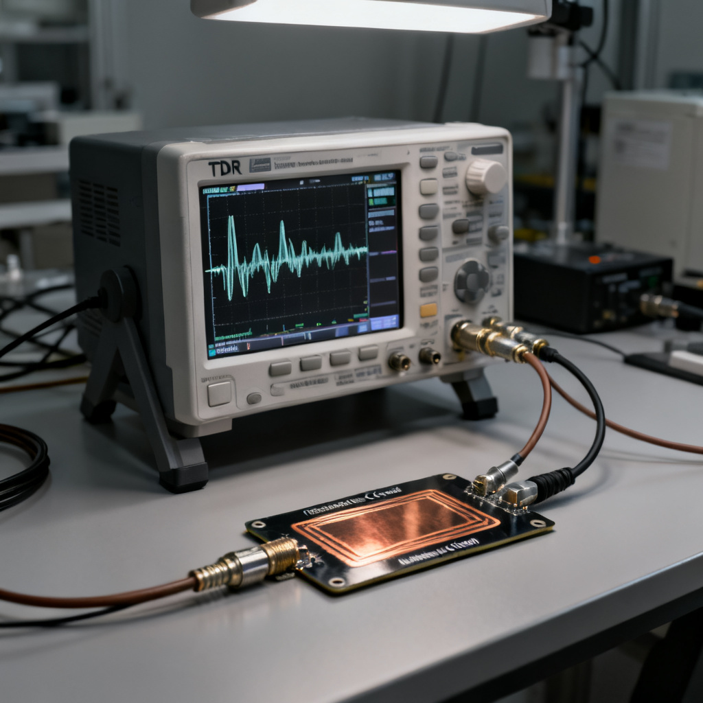
Post-Manufacturing Validation
Always include dedicated impedance test coupons that mimic the actual board’s stackup, solder mask, and surface finish. Use Time Domain Reflectometry (TDR) to measure actual impedance. A deviation of more than ±2 ohms indicates a need to adjust compensation factors. Work with your fabricator to track impedance data across multiple batches using Statistical Process Control (SPC).
When to Use SMD vs. NSMD Pads
Avoid Solder Mask Defined (SMD) pads for impedance-critical traces as they introduce discontinuities. Use Non-Solder Mask Defined (NSMD) pads, which reduce the solder mask’s influence on pad impedance.
Industry Best Practices and Common Pitfalls
Best Practices for Impedance Control PCB Accuracy
Communicate with your fabricator: provide explicit instructions for solder mask thickness (target 0.3–0.5 mil over traces) and surface finish type. Use low-Dk solder mask (Dk 3.3–3.5) for high-frequency designs. Avoid black solder mask on high-speed traces. Select OSP for impedance-critical outer layers. If OSP is not possible, use Immersion Silver and ensure thickness is tightly controlled. Account for both layers in simulation—never simulate impedance without including solder mask.
Common Pitfalls
Assuming solder mask has no effect is the #1 mistake. Using default solder mask parameters in solvers (0 mil thickness or generic Dk) is another. Ignoring surface finish for internal layers is acceptable, but for outer layers it is critical. Not testing with the actual finish—impedance coupons with bare copper will not reflect real-world impedance.
Conclusion: Precision Requires Holistic Modeling
Achieving accurate impedance control PCB accuracy demands that you treat solder mask and surface finish as integral parts of the transmission line. Solder mask reduces impedance due to its higher dielectric constant, while surface finishes like ENIG can increase impedance due to the nickel layer’s lower conductivity and magnetic properties. Their combined effect can cause a 2–8 ohm deviation from the target. To ensure your designs meet required impedance tolerance (typically ±10% or ±5% for high-speed), model both layers in your field solver, compensate trace geometry accordingly, select the right finish (OSP is best, ENIG requires compensation), and validate with TDR on production-quality coupons.
FAQ: How Solder Mask and Surface Finish Affect Impedance Control PCB Accuracy
What is the main effect of solder mask on impedance control PCB accuracy?
Solder mask reduces impedance because its dielectric constant (Dk 3.3–4.5) is higher than air, increasing the effective dielectric constant of the transmission line.
Which surface finish is best for maintaining impedance control PCB accuracy?
OSP (Organic Solderability Preservative) is best because it is an insulator and does not alter copper’s electrical properties, making it ideal for high-speed designs.
How much can ENIG change impedance control PCB accuracy?
ENIG can increase impedance by +1 to +3 ohms due to the nickel layer’s lower conductivity and ferromagnetic properties.
Can solder mask color affect impedance control PCB accuracy?
Yes, black solder mask has a higher Dk (4.0–4.5) and higher loss tangent, leading to greater impedance reduction and signal attenuation compared to green mask.
How do I compensate for solder mask and surface finish in my design?
Use a field solver to model both layers, adjust trace width (increase for solder mask, decrease for ENIG), and increase dielectric height if needed. Always validate with TDR on production coupons.
“`