Impedance control PCB stackup design is the foundation of high-speed signal integrity, ensuring reliable performance in B2B electronics. This guide provides a comprehensive workflow for building controlled impedance stackups in Altium Designer, Cadence Allegro, and KiCad, covering theory, material selection, and tool-specific steps.
Section 1: Fundamentals of Impedance Control PCB Stackup Design
1.1 What is Controlled Impedance in PCB Stackup?
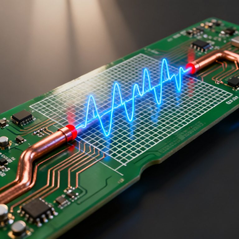
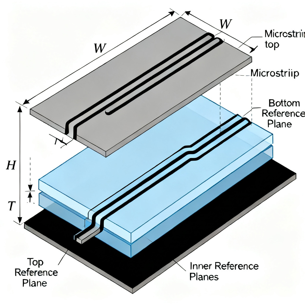
Controlled impedance (Z₀) is the characteristic impedance of a transmission line, measured in ohms (Ω). For high-speed signals, the target is typically 50 Ω (single-ended) or 100 Ω (differential). The impedance control PCB stackup design ensures that the signal path has a consistent impedance from driver to receiver, minimizing reflections.
The key parameters affecting impedance include:
- Trace width (W): Wider traces lower impedance.
- Dielectric height (H): Thicker dielectric increases impedance.
- Copper thickness (T): Thicker copper slightly reduces impedance.
- Dielectric constant (Dk or εr): Higher Dk lowers impedance.
- Solder mask and surface finish: These can slightly alter impedance (usually by 2-5 Ω).
Important: Impedance is determined by the physical stackup, not the schematic. Thus, stackup design must precede routing.
1.2 Types of Transmission Lines in Impedance Control PCB Stackup
- Microstrip: A trace on an outer layer with a reference plane below. Common for top/bottom layers.
- Stripline: A trace on an inner layer sandwiched between two reference planes. Offers better shielding but is harder to manufacture.
- Differential Pairs: Two traces with controlled spacing (S) to achieve a specific differential impedance (Z_diff). For 100 Ω differential, Z_diff ≈ 2 × Z₀ (if tightly coupled).
1.3 Key Stackup Variables for Impedance Control PCB Stackup
From manufacturing perspective, the stackup must be symmetric to prevent warpage. For impedance control:
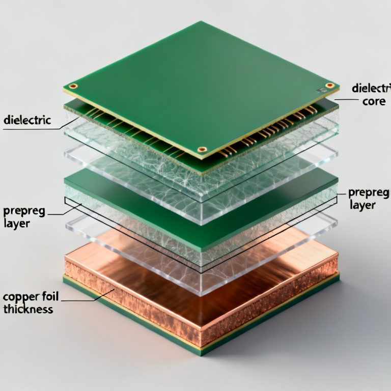
- Core vs. Prepreg: Core is cured material with fixed thickness; prepreg is semi-cured and compresses during lamination. Use core for precise impedance layers.
- Copper weight: 0.5 oz, 1 oz, or 2 oz. Thicker copper reduces impedance but complicates etching.
- Dielectric material: FR-4 (Dk ~4.2-4.5), high-speed laminates (e.g., Rogers, Isola), or low-loss materials for RF.
Rule of thumb: For 50 Ω microstrip on standard FR-4 (Dk=4.2, H=0.2 mm, T=0.035 mm), trace width ≈ 0.35 mm.
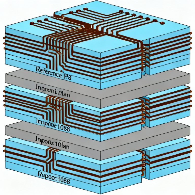
Section 2: Building Impedance Control PCB Stackup in Altium Designer
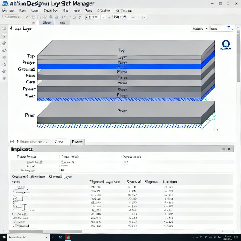
2.1 Setting Up the Layer Stack Manager for Impedance Control PCB Stackup
Altium Designer provides a powerful Layer Stack Manager (Design → Layer Stack Manager). Follow these steps:
- Define Layer Count and Type: Add layers (e.g., 4-layer: Top, GND, PWR, Bottom). Set layer type: Signal, Plane (for power/ground), or Dielectric. Use “Internal Plane” for solid copper layers (e.g., GND and PWR).
- Configure Material Properties: For each dielectric layer, enter: Material name (e.g., FR-4, Rogers 4350B), Dielectric constant (Dk) (use manufacturer data, e.g., FR-4: 4.2 @ 1 GHz), Dielectric thickness (H) (in mm or mils), Loss tangent (Df) (optional for high-frequency analysis). For conductive layers, set copper thickness (e.g., 1 oz = 0.035 mm).
- Impedance Calculation: In the Layer Stack Manager, click Impedance tab. Select trace type: Microstrip or Stripline. Enter target impedance (e.g., 50 Ω). Altium calculates required trace width and spacing based on stackup. Adjust dielectric height or width until impedance matches.
Pro Tip: Use the “Symmetric” option to ensure balanced stackup (e.g., Top and Bottom same thickness, inner layers symmetric).
2.2 Defining Impedance Rules for Routing in Impedance Control PCB Stackup
- Go to Design → Rules → Routing → Width.
- Create a new rule (e.g., “50_Ohm_Trace”).
- Set Min/Max/Preferred Width to the calculated value (e.g., 0.35 mm).
- Use Query Builder to target specific nets (e.g.,
InNet(‘CLK’)orIsDifferentialPair). - For differential pairs, create a Differential Pairs Routing rule: Set Min/Max Gap and Primary Gap (e.g., 0.2 mm). Enable “Max Uncoupled Length” to avoid impedance discontinuities.
2.3 Verifying with 3D and Signal Integrity for Impedance Control PCB Stackup
- Use Tools → Signal Integrity to simulate reflections and crosstalk.
- Altium’s Impedance Profiler (Pro version) can analyze real-time impedance during routing.
Section 3: Building Impedance Control PCB Stackup in Cadence Allegro
3.1 Using the Cross-Section Editor for Impedance Control PCB Stackup
Cadence Allegro’s Cross-Section Editor (Setup → Cross-Section) is the core tool for stackup design.
- Add Physical Layers: Define Subclass Name (e.g., TOP, GND, SIG1, SIG2, BOTTOM). Set Type: CONDUCTOR, PLANE, or DIELECTRIC. For dielectric layers, input Material Name and Thickness.
- Assign Material Properties: Use Material Manager (Setup → Materials) to define Dk, Df, and conductivity. Common materials: FR-4 (Dk=4.2), Polyimide (Dk=3.5), Rogers (Dk=3.0-10.2). For copper, set Conductivity (5.8e7 S/m for standard copper).
- Impedance Calculation: Click Impedance tab in Cross-Section Editor. Choose Single-Ended or Differential. Enter target impedance (e.g., 50 Ω). Adjust trace width (W) and dielectric height (H) until impedance matches. Cadence shows calculated impedance for each layer in real-time.
Advanced: Use “Stackup Wizard” for multi-layer high-speed designs (e.g., 8-layer with multiple reference planes).
3.2 Setting Up Constraint Regions for Impedance Control PCB Stackup
- Open Constraint Manager (Setup → Constraints → Constraint Manager).
- Create Physical Constraint Set (e.g., “50_OHM”): Set Minimum Line Width to calculated value. For differential pairs, create a Differential Pair Constraint with Primary Gap and Tolerance.
- Assign constraint sets to specific nets using Net Class or Property (e.g.,
SIG_CLASS).
3.3 Manufacturing Output and DFM Checks for Impedance Control PCB Stackup
- Use Manufacturing → Artwork to generate Gerber files with impedance labels.
- Enable DFM (Design for Manufacturing) checks: Minimum annular ring for vias, Copper balancing to prevent warpage.
- Cadence’s Sigrity tool can perform 3D electromagnetic simulation for impedance validation.
Section 4: Building Impedance Control PCB Stackup in KiCad
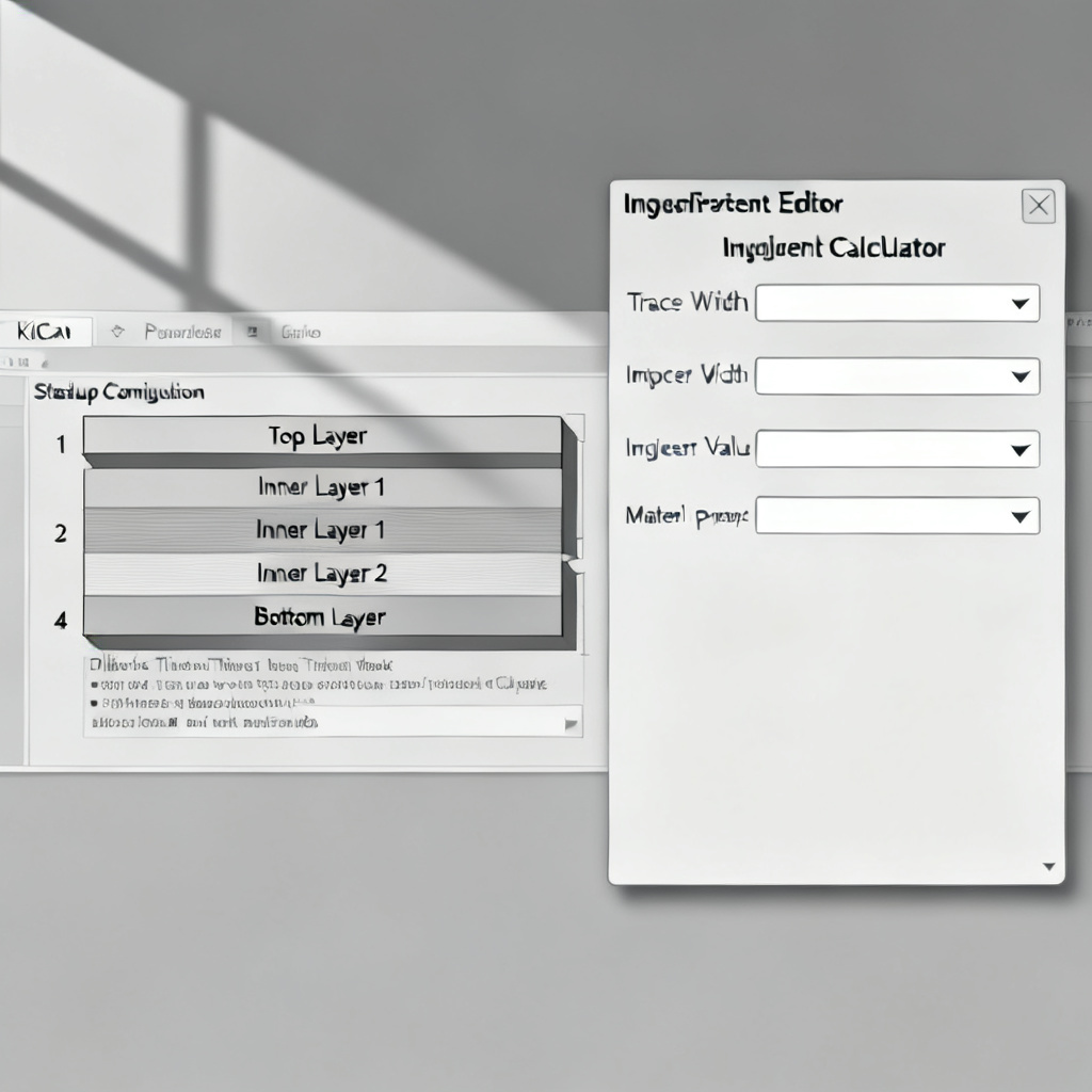
4.1 Configuring Board Stackup in PCB Editor for Impedance Control PCB Stackup
KiCad’s Board Setup (File → Board Setup → Stackup) is straightforward but powerful.
- Add Layers: Click “Add Layer” for each physical layer. Set Type: F.Cu (top copper), In1.Cu, In2.Cu, B.Cu (bottom copper). Add dielectric layers between copper layers.
- Define Material Parameters: For each dielectric, enter: Thickness (e.g., 0.2 mm), Dielectric Constant (e.g., 4.5 for standard FR-4), Loss Tangent (optional, e.g., 0.02). KiCad supports material libraries (e.g., FR-4, Rogers 4003C).
- Impedance Calculation: KiCad has a built-in Impedance Calculator (Tools → Impedance Calculator). Choose Microstrip or Stripline. Input Trace Width, Dielectric Height, Copper Thickness, and Dk. KiCad displays calculated impedance (Z₀) and differential impedance (Z_diff). Adjust width until target is met.
Note: KiCad does not automatically update stackup based on target impedance—you must iterate manually. For complex designs, use external calculators (e.g., Saturn PCB Toolkit) and then input values.
4.2 Applying Impedance Rules to Routing in Impedance Control PCB Stackup
- Go to Board Setup → Design Rules → Net Classes.
- Create a net class (e.g., “50_Ohm”).
- Set Track Width to the calculated value.
- For differential pairs, create a separate net class with Track Width and Clearance (gap).
- Assign nets to classes via Schematic → Annotate or PCB Editor → Assign Net Class.
Tip: Use “Differential Pair” routing mode (Route → Differential Pair) and set gap via net class clearance.
4.3 Verification and Export for Impedance Control PCB Stackup
- Use Inspect → Measure to verify trace widths.
- Run DRC (Design Rule Check) to ensure no violations.
- Export Gerber files with impedance notes (e.g., “50 Ω impedance controlled”).
Section 5: Common Pitfalls and Best Practices in Impedance Control PCB Stackup
5.1 Stackup Symmetry and Warpage
- Pitfall: Asymmetric stackup (e.g., thick copper on one side only) causes board warpage during reflow.
- Fix: Mirror copper thickness and dielectric layers. For 4-layer boards, use same prepreg/core thickness on top and bottom.
5.2 Impedance Tolerance in Manufacturing
- Pitfall: Assuming theoretical impedance matches production. Actual impedance can vary ±10% due to etching, lamination pressure, and Dk tolerance.
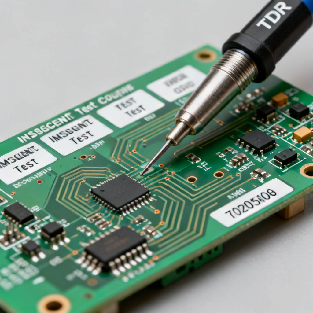
- Fix: Request impedance coupons from your PCB manufacturer. Coupons are test strips on the panel that measure actual impedance. Specify tolerance (e.g., ±5 Ω for 50 Ω).
5.3 Via Impact on Impedance
- Pitfall: Vias create impedance discontinuities (capacitive or inductive).
- Fix: Use back-drilling for high-speed signals to remove unused via stubs. For critical traces, avoid vias altogether or use microvias.
5.4 Solder Mask and Surface Finish
- Pitfall: Solder mask (Dk ~3.5-4.0) lowers impedance by 2-5 Ω.
- Fix: Include solder mask thickness in impedance calculations (Altium and Cadence allow this). Use ENIG or OSP finish for minimal impact.
5.5 Cross-Tool Consistency
- Pitfall: Different EDA tools may calculate impedance differently due to formulas (e.g., IPC-2141 vs. empirical models).
- Fix: Use a single reference calculator (e.g., Saturn PCB Toolkit) for all tools. Verify with manufacturer’s stackup.
Section 6: Case Study: 8-Layer High-Speed Impedance Control PCB Stackup
6.1 Stackup Design for Impedance Control PCB Stackup
For a typical high-speed digital board (e.g., 10 Gbps Ethernet):
| Layer | Type | Material | Thickness (mm) | Copper (oz) |
|---|---|---|---|---|
| L1 (Top) | Signal | FR-4 | 0.2 | 0.5 |
| L2 | GND | FR-4 core | 0.1 | 1 |
| L3 | Signal | Prepreg | 0.3 | 0.5 |
| L4 | PWR | Core | 0.1 | 1 |
| L5 | GND | Core | 0.1 | 1 |
| L6 | Signal | Prepreg | 0.3 | 0.5 |
| L7 | PWR | Core | 0.1 | 1 |
| L8 (Bottom) | Signal | FR-4 | 0.2 | 0.5 |
Impedance control targets: 50 Ω single-ended (microstrip on L1, L8; stripline on L3, L6), 100 Ω differential.
6.2 Tool-Specific Implementation for Impedance Control PCB Stackup
- Altium: Use Layer Stack Manager with symmetric option. Add impedance rules for each signal layer.
- Cadence: Define constraint sets for each net class. Use Sigrity for simulation.
- KiCad: Manually calculate widths using impedance calculator, then assign net classes.
6.3 Manufacturing Notes for Impedance Control PCB Stackup
- Specify controlled impedance on fabrication drawing.
- Request coupon test for each impedance target.
- Use high-speed laminate (e.g., Isola FR408) for L3 and L6 to reduce loss.
FAQ: Impedance Control PCB Stackup
What is impedance control PCB stackup design?
Impedance control PCB stackup design is the process of defining layer materials, thicknesses, and trace geometries to achieve a specific characteristic impedance (e.g., 50 Ω) for high-speed signals, ensuring signal integrity in PCBs.
How do I calculate impedance for PCB stackup in Altium?
In Altium Designer, use the Layer Stack Manager’s Impedance tab. Select trace type (microstrip/stripline), enter target impedance, and adjust dielectric height or trace width until the calculated impedance matches your requirement for impedance control PCB stackup.
What is the difference between microstrip and stripline in impedance control PCB stackup?
Microstrip is a trace on an outer layer with one reference plane, while stripline is an inner-layer trace between two planes. Stripline offers better shielding but is harder to manufacture for impedance control PCB stackup.
Can KiCad handle impedance control PCB stackup design?
Yes, KiCad includes an Impedance Calculator tool for microstrip and stripline. You manually input stackup parameters and adjust trace width to achieve target impedance for impedance control PCB stackup. It does not auto-calculate from target, so external tools may help.
Why is stackup symmetry important in impedance control PCB stackup?
Asymmetric stackups cause board warpage during reflow, leading to impedance variations. Symmetric copper and dielectric layers ensure consistent impedance control PCB stackup performance and manufacturing reliability.
“`