Mastering impedance control PCB for flex and rigid-flex designs is essential for high-speed signal integrity in modern electronics. As data rates climb into the GHz range, even minor mismatches can cause reflections, signal degradation, and electromagnetic interference (EMI). This challenge intensifies when transitioning from rigid to flexible substrates. Flex and rigid-flex PCBs introduce unique variables—dynamic bending, thinner dielectrics, and material anisotropy—that complicate impedance control. This pillar page consolidates the best practices from industry leaders to help you design flex circuits with precise impedance tolerances (±5% to ±10%), ensuring reliable performance in applications like aerospace, medical devices, and 5G communications.
Fundamentals of Impedance Control in Flexible Circuits for Impedance Control PCB
What is Characteristic Impedance?
Characteristic impedance (Z₀) is the opposition a transmission line offers to a signal traveling along it. For a microstrip or stripline on a flex PCB, Z₀ depends on trace width (W) and thickness (T), dielectric constant (Dk) of the substrate (e.g., polyimide, LCP), distance from the reference plane (H) – critical in thin flex layers, and solder mask and coverlay effects (coverlay reduces impedance by 2–5 ohms typically). Unlike rigid FR4, flex materials like polyimide have a lower and more stable Dk (3.0–3.5 at 1 GHz), but the Dk varies with bending radius. Always simulate in both flat and bent states.
Why Flex Impedance Control is Different for Impedance Control PCB
Three critical distinctions from rigid PCBs exist: thinner dielectrics (flex cores are 12.5–50 µm thick, making impedance more sensitive to trace width variations), coverlay vs. solder mask (coverlay has a different Dk than solder mask, requiring separate impedance models), and dynamic bending (impedance can shift 2–8% during flexing due to mechanical strain on copper traces). Use “impedance coupons” (test structures) on the panel edge to verify Z₀ before assembly. For rigid-flex, include coupons on both rigid and flex sections.
Material Selection for Controlled Impedance Flex PCBs for Impedance Control PCB
Core Materials: Polyimide vs. LCP vs. Modified Epoxy
| Material | Dk (1 GHz) | Df (Loss Tangent) | Flexibility | Best For |
|---|---|---|---|---|
| Standard Polyimide (e.g., Kapton) | 3.4–3.5 | 0.002–0.005 | Excellent | General high-speed flex |
| Liquid Crystal Polymer (LCP) | 2.9–3.1 | 0.0015–0.002 | Good | Millimeter-wave / RF |
| Modified Epoxy (e.g., FR4 flex grade) | 4.0–4.5 | 0.01–0.02 | Moderate | Cost-sensitive rigid-flex |
LCP offers the best high-frequency performance due to low moisture absorption (0.04%) and stable Dk across humidity. Polyimide with low-flow adhesive reduces impedance variation during lamination. Avoid standard FR4 for flex sections – its higher Dk and loss degrade signal integrity above 3 GHz.
Copper Foil: Rolled Annealed vs. Electrodeposited
Rolled Annealed (RA) copper is preferred for dynamic flexing; its smoother surface reduces skin effect losses at high frequencies. Electrodeposited (ED) copper has higher surface roughness (Rz ~2–5 µm) which increases conductor loss by 10–15% at 10 GHz, so use only for static flex. All three top articles emphasize that copper roughness directly impacts impedance accuracy. RA copper yields tighter impedance control (±5% vs. ±8% for ED) in thin dielectrics.
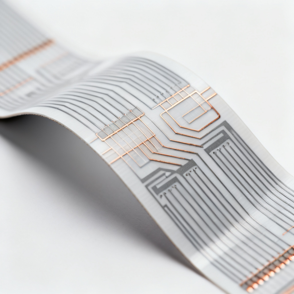
Coverlay and Bonding Adhesives
Coverlay is not just a protective layer – it is part of the transmission line. Key parameters include thickness (12.5–25 µm polyimide + 12.5–25 µm adhesive, total 25–50 µm), adhesive Dk (acrylic adhesives Dk ~3.2–3.5 vs. epoxy Dk ~3.8–4.2), and impedance impact (a 25 µm coverlay can reduce Z₀ by 3–7 ohms compared to bare copper). Specify “impedance-controlled coverlay” with known Dk and thickness tolerance (±2 µm). Request the manufacturer’s coverlay Dk data sheet.
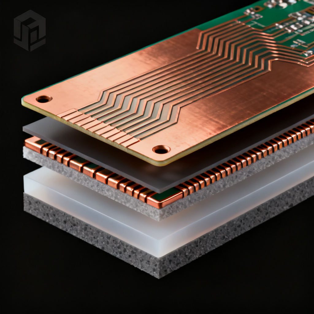
Stack-Up Design for Flex and Rigid-Flex Impedance Control for Impedance Control PCB
Microstrip vs. Stripline in Flex
Microstrip (outer layer) is easier to manufacture but more susceptible to EMI and coverlay effects, ideal for single-layer flex. Stripline (embedded layer) provides better isolation and impedance stability but requires two reference planes, preferred for multi-layer rigid-flex. For microstrip on polyimide (Dk=3.5, H=50 µm, T=18 µm), typical trace width for 50 ohms is 80–120 µm depending on coverlay.
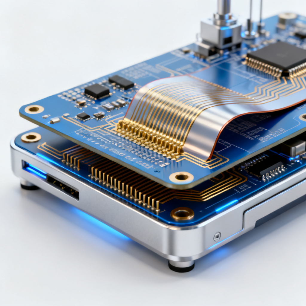
Asymmetric Stack-Ups in Rigid-Flex
Rigid-flex often has different layer counts in rigid and flex sections. Maintain continuous reference planes across the rigid-flex boundary. Use “dogbone” or “teardrop” transitions to avoid impedance discontinuities at the bend.
Via Design for Impedance Matching
Vias in flex are a major source of impedance mismatch. Use microvias (laser-drilled) for thin flex layers – they have lower parasitic capacitance. Via diameter should be 150–200 µm for 50 ohm transitions. Back-drill through-hole vias in rigid sections to remove stub effects above 5 GHz. For rigid-flex, avoid plated through-holes in the dynamic flex area; use “flexible via” designs (e.g., staggered microvias) to prevent stress fractures.
Manufacturing Tolerances and Impedance Verification for Impedance Control PCB
Key Tolerances That Affect Impedance
| Parameter | Typical Tolerance | Impact on Z₀ (50 ohm line) |
|---|---|---|
| Trace width (W) | ±10 µm | ±2–3 ohms |
| Dielectric thickness (H) | ±10% | ±3–5 ohms |
| Copper thickness (T) | ±5 µm | ±1–2 ohms |
| Coverlay thickness | ±5 µm | ±1–2 ohms |
| Dk variation | ±0.1 | ±1–2 ohms |
Total Impedance Tolerance is ±8–10% for standard flex, ±5% for premium (with RA copper and tight process control).
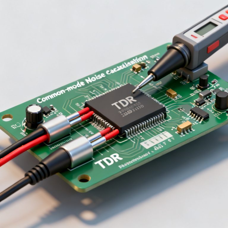
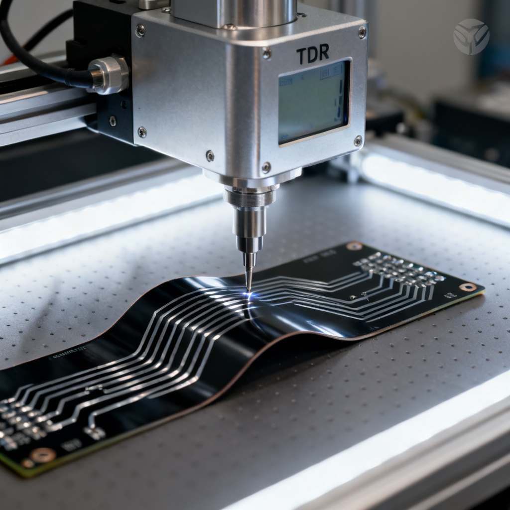
TDR (Time Domain Reflectometry) Testing
All three top articles recommend TDR as the gold standard for verification. Test coupons should be placed at panel edges and near critical flex bends. Acceptance criteria: Z₀ within ±5% of target for high-speed signals (e.g., 50 ohms ±2.5 ohms). For rigid-flex, test both rigid and flex sections separately, plus the transition zone. Request “impedance test reports” from your fabricator; look for correlation between simulated and measured values – discrepancies >5% indicate process issues.
Common Defects and Solutions
If impedance is too low, it is caused by over-etching (narrow traces) or too-thin dielectric; solution: increase trace width by 5–10 µm in the design. If impedance is too high, it is caused by under-etching or thick dielectric; solution: reduce dielectric thickness or use higher Dk material. Variation across panel often results from uneven lamination pressure; solution: use “low-flow” adhesive and matched impedance laminates.
Design for Manufacturability (DFM) Rules for Impedance Control PCB
Trace and Space Guidelines
Minimum trace width is 75 µm (for 50 ohms with 50 µm dielectric). Minimum space to adjacent signals is 100 µm (to avoid crosstalk). Copper weight: 0.5 oz (18 µm) for dynamic flex; 1 oz (35 µm) for static flex.
Bend Radius and Impedance
For dynamic flex, bend radius ≥ 10× the total flex thickness (e.g., for 200 µm stack, R ≥ 2 mm). Impedance change during bending is typically 2–5% increase in Z₀ for concave bends (inner radius compresses dielectric). Use 3D EM solvers (e.g., Ansys HFSS) to model bent states.
Layer Transition Management
Use staggered transitions to avoid abrupt layer changes; apply gradual tapers over 2–3 mm. Maintain symmetrical copper distribution to prevent warpage. Use “no-flow” prepreg in rigid-flex bonding areas to prevent resin bleed into flex zones.
Advanced Topics for High-Speed Flex Design for Impedance Control PCB
Differential Impedance for Flex
For high-speed pairs (USB 3.0, HDMI, PCIe), target 100 ohms differential (90 ohms for USB). Design rule: spacing between pair = 2× trace width (e.g., 200 µm for 100 µm traces). Keep pair geometry constant through bends; avoid skew >5 ps.
Impedance Control for Multi-Layer Rigid-Flex
Challenges include layer-to-layer registration (±50 µm misalignment can shift impedance by 3–5 ohms), via stub effects (in 12+ layer rigid-flex, use back-drilling or blind vias), and thermal management (high-speed signals generate heat; use thermal vias in rigid sections).
Simulation Workflow
Pre-layout: use 2D field solver (e.g., Polar SI9000) with material Dk from IPC-4101C. Post-layout: 3D EM simulation of critical nets (especially rigid-flex transitions). Manufacturing: send simulated stack-up to fabricator for correlation. Validation: TDR measurement of test coupons plus final assembly.
Why Choose Our High-Speed Flex & Rigid-Flex PCBs for Impedance Control PCB
At [Your Company Name], we specialize in impedance-controlled flex and rigid-flex PCBs for demanding high-speed applications. Our capabilities include tight tolerances (±5% impedance control on 50–100 ohm lines), material expertise (polyimide, LCP, and hybrid stacks with verified Dk/Df data), advanced testing (TDR on every panel, with full impedance reports), rigid-flex integration (seamless transitions up to 20+ layers), and lead time (5–7 days for prototypes, 15–20 days for production). Request your custom impedance profile by contacting our engineering team for a free stack-up simulation and DFM review.
Frequently Asked Questions About Impedance Control PCB for Flex and Rigid-Flex Designs
Can I achieve 50 ohms on a single-layer flex without a ground plane for impedance control PCB?
How does bending affect impedance over time in impedance control PCB designs?
What is the maximum frequency for impedance-controlled flex in an impedance control PCB?
Do I need impedance control for all flex signals in an impedance control PCB?
Mastering impedance control PCB for flex and rigid-flex designs requires a holistic approach: careful material selection, precise stack-up design, rigorous manufacturing tolerances, and thorough testing. By applying the principles from this guide—leveraging the expertise of industry leaders—you can achieve first-pass success in your high-speed flexible circuit designs. Ready to start your project? Contact our engineers for a personalized consultation.
“`