Master impedance control PCB calculation using Polar Si9000 with this definitive step-by-step guide for high-speed PCB design. In high-speed digital design, signal integrity is paramount; even minor mismatches cause reflections and EMI. This guide covers stackup, trace geometry, differential pairs, and practical tips to achieve reliable controlled impedance.
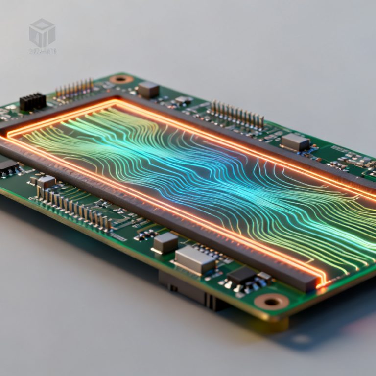
Why impedance control matters: Characteristic impedance (Z₀) is not a property of the trace alone—it depends on the entire transmission line structure. Key variables include trace width (W), trace thickness (T), dielectric height (H), dielectric constant (Dk), and solder mask thickness. Common impedance types are single-ended (50Ω, 75Ω) and differential (90Ω, 100Ω, 110Ω).
Fundamentals of Impedance Control PCB Calculation
Key Variables Influencing Impedance Control PCB Calculation
- Trace Width (W): Wider traces lower impedance; narrower traces raise it.
- Trace Thickness (T): Heavier copper reduces impedance slightly due to increased capacitance.
- Dielectric Height (H): Distance from signal layer to reference plane—larger height increases impedance.
- Dielectric Constant (Dk): Relative permittivity of substrate—higher Dk lowers impedance.
- Solder Mask Thickness: Can lower impedance by 3–8 ohms for fine geometries.
Common Impedance Types in Impedance Control PCB Calculation
- Single-Ended (Microstrip/Stripline): Single trace over a reference plane. Standard: 50Ω, 75Ω.
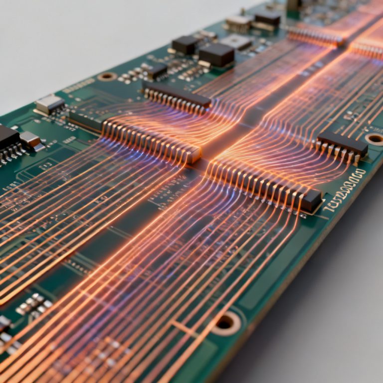
- Differential (Edge-Coupled): Two traces with specific spacing. Common: 90Ω (USB), 100Ω (Ethernet), 110Ω (LVDS).
- Coplanar Waveguide: Trace with ground planes on same layer, used for RF.
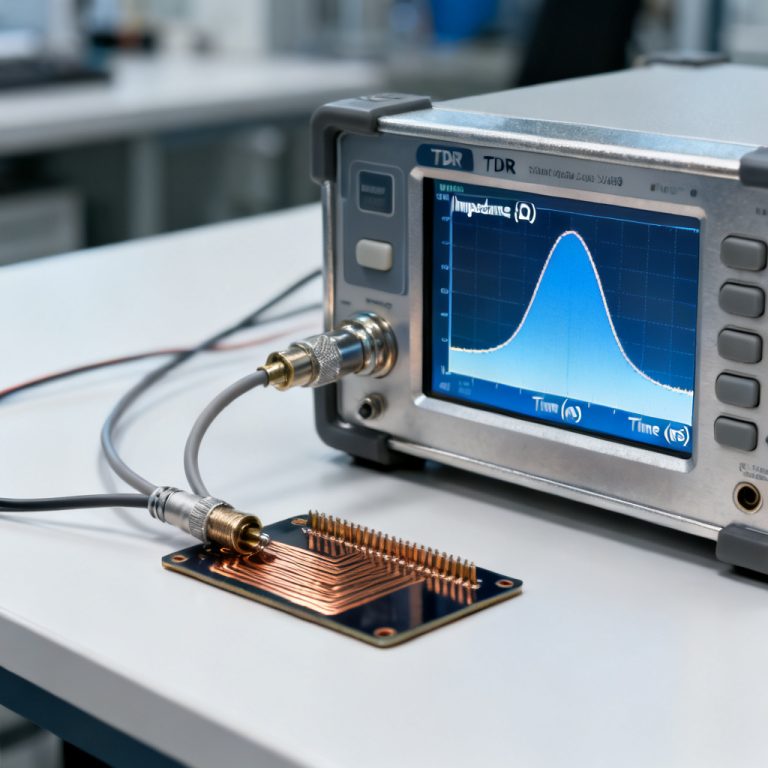
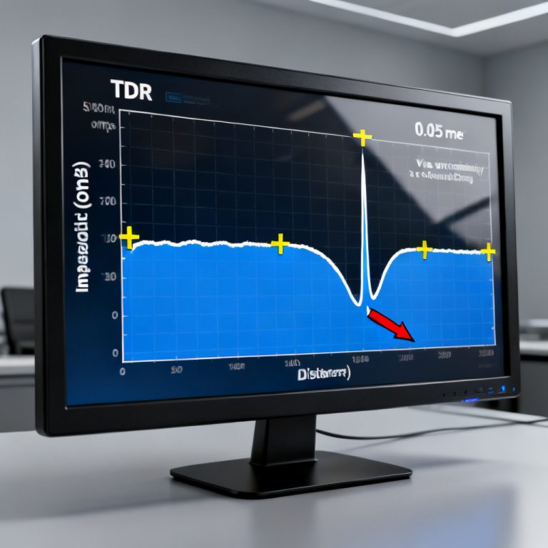
Pro Tip: Always request a controlled impedance coupon on your PCB panel for TDR verification before full production.
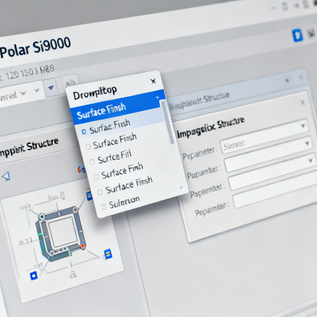
Setting Up Polar Si9000 for Impedance Control PCB Calculation
Step 1: Select Correct Surface Finish
Navigate to the Surface Finish dropdown in Polar Si9000. Options include HASL, ENIG, Immersion Silver, and OSP. ENIG adds nickel under gold, increasing trace thickness. Selecting the correct finish ensures the calculator accounts for final copper thickness after plating.
Step 2: Choose the Impedance Structure
From the left panel, select your structure: Surface Microstrip (Single-Ended), Surface Microstrip (Differential), Offset Stripline (Single-Ended), Edge-Coupled Offset Stripline, or Asymmetric Stripline. For high-speed designs, stripline is preferred over microstrip because it is shielded by two planes, reducing EMI.
Step-by-Step: Single-Ended 50Ω Microstrip Impedance Control PCB Calculation
Step 1: Enter Physical Parameters
- Dielectric Constant (Er): 4.2 (typical for FR-4 at 1GHz).
- Dielectric Height (H1): 4 mils (core thickness between Layer 1 and Layer 2).
- Trace Width (W): Start at 5 mils.
- Trace Thickness (T): 1.4 mils (1 oz copper + plating).
- Solder Mask Thickness (C1, C2): 0.5 mils.
Step 2: Click Calculate
The software returns impedance. If not 50Ω, iterate by adjusting width in 0.5 mil increments. Use the Target Impedance feature (Options > Target Impedance) to solve for required width automatically.
Step 3: Check Solder Mask Effect
Toggle solder mask parameter on/off—you will see a 3–5Ω drop when applied. Many fabs ask for bare copper impedance and adjust mask thickness. Always clarify with your supplier.
Critical Warning: Run a parametric sweep to see how impedance changes over ±10% tolerance in dielectric height and trace width. This reveals your process window.
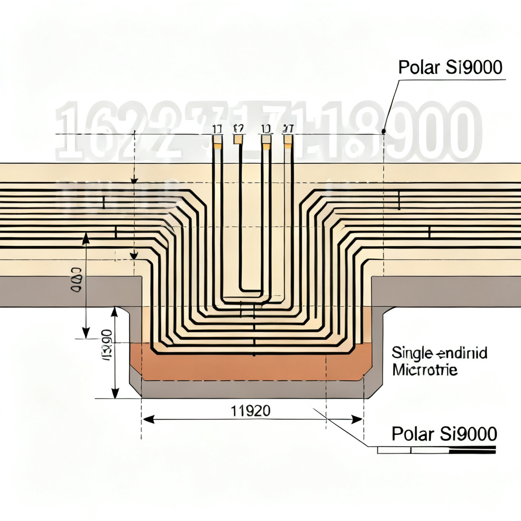
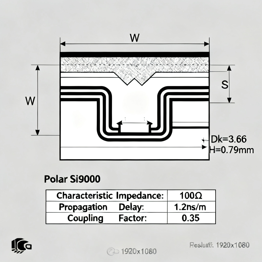
Step-by-Step: Differential 100Ω Stripline Impedance Control PCB Calculation
Step 1: Select Structure
Choose Edge-Coupled Offset Stripline.
Step 2: Enter Parameters
- Dielectric Constant (Er): 4.0 (inner layer prepreg).
- Distance to Upper Plane (H1): 5 mils.
- Distance to Lower Plane (H2): 5 mils.
- Trace Width (W): Start at 4 mils.
- Trace Spacing (S): Start at 6 mils (edge-to-edge).
- Trace Thickness (T): 1.2 mils.
Step 3: Calculate and Interpret
The software shows Odd-Mode Impedance (Zodd) and Differential Impedance (Zdiff). Zdiff = 2 × Zodd. For 100Ω differential, Zodd should be 50Ω. Increasing spacing (S) reduces coupling and increases Zdiff; decreasing spacing increases coupling and lowers Zdiff.
Step 4: Optimize for Tight Tolerance
Use the Differential Pair Wizard to find W and S that yield target Zdiff while maintaining manufacturable gap (S ≥ 1.5× W). Edge-coupled is easier to manufacture than broadside coupled.
Advanced Considerations in Impedance Control PCB Calculation
Frequency-Dependent Dielectric Constant (Dk)
FR-4 Dk drops from ~4.5 at 1 MHz to ~4.0 at 10 GHz. Use the Material Library in Si9000 to select pre-characterized laminates (e.g., Isola 370HR, Rogers 4350B). Never assume Dk is constant.
Copper Roughness Correction
Rough copper increases conductor losses. Si9000 has a Surface Roughness model (e.g., Hammerstad or Huray). Enable it for designs above 5 GHz.
Etch Factor
Etching produces trapezoidal traces. Si9000 can model this as Trapezoidal profile. Ask your PCB fab for their typical etch factor (e.g., 2:1) for more accurate calculation.
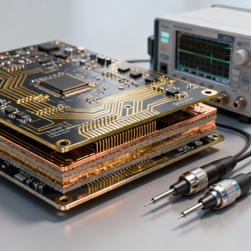
Verification & Integration of Impedance Control PCB Calculation
Export Stackup to CAD
In Si9000, go to File > Export > Stackup and save as .CSV or .XML. Import into your layout tool (Altium, Cadence Allegro, KiCad) to ensure design rules match calculated dimensions.
Generate Impedance Tables
Use the Table Generator in Si9000 to create a table of exact W and S for each layer and target. Provide this table to your manufacturer as part of the fabrication drawing.
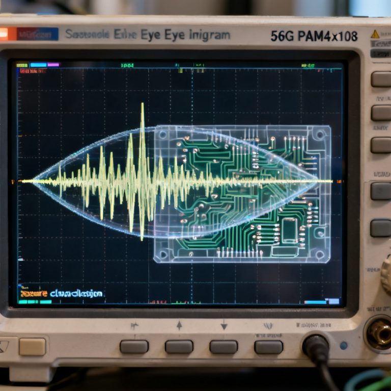
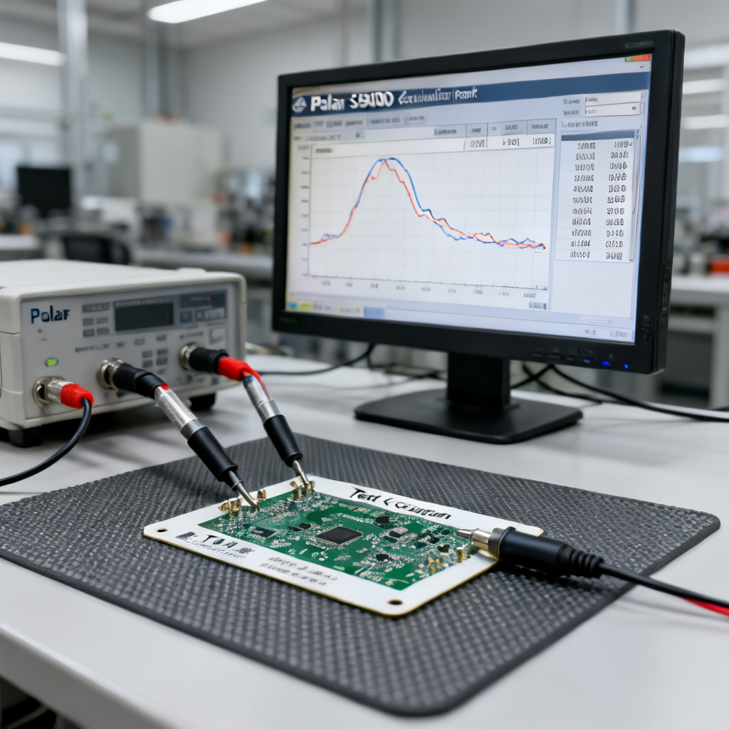
TDR Verification on Prototype
Request TDR testing on the impedance coupon. Compare measured impedance to Si9000 calculation. A difference of ±5% is typical for FR-4; ±2% is achievable with high-end laminates.
Final Expert Advice: Cross-check a single calculation with the IPC-2141A approximation for microstrip: Z₀ ≈ 87/√(Er+1.41) × ln(5.98H/(0.8W+T)). This helps catch gross errors.
Impedance Control PCB Calculation: Comparison Table
| Parameter | Single-Ended 50Ω Microstrip | Differential 100Ω Stripline |
|---|---|---|
| Trace Width (W) | 5 mils (typical) | 4 mils (typical) |
| Trace Spacing (S) | N/A | 6 mils (edge-to-edge) |
| Dielectric Height (H) | 4 mils | 5 mils each side |
| Dielectric Constant (Er) | 4.2 | 4.0 |
| Trace Thickness (T) | 1.4 mils | 1.2 mils |
| Solder Mask Effect | 3–5Ω drop | Minimal (inner layer) |
FAQ: Impedance Control PCB Calculation Using Polar Si9000
What is the first step in impedance control PCB calculation using Polar Si9000?
The first step is selecting the correct surface finish and impedance structure (e.g., microstrip or stripline) based on your PCB layer stackup.
How does solder mask affect impedance control PCB calculation?
Solder mask can lower impedance by 3–8 ohms for fine geometries. Always model it in Polar Si9000 for accurate results.
Why is differential impedance important in impedance control PCB calculation?
Differential impedance (e.g., 100Ω for Ethernet) ensures signal integrity in high-speed differential pairs by matching source and load impedances.
What is the target impedance feature in Polar Si9000?
The Target Impedance feature automatically solves for trace width to achieve a specified impedance, streamlining the design process.
How do I verify impedance control PCB calculation results?
Request TDR testing on a controlled impedance coupon and compare measured values to Polar Si9000 calculations.
“`