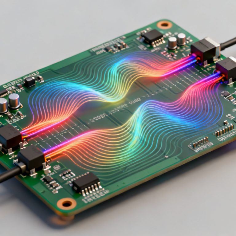
In high-speed PCB design, accurate Reflection in Transmission Line Measurement Using VNA (S11 Return Loss) is critical for signal integrity. This guide provides a complete methodology for measuring and interpreting S11 return loss in high-speed PCBs, ensuring impedance control and compliance with modern standards like PCIe Gen5.
Fundamentals of Reflection in Transmission Line Measurement Using VNA
What is Reflection in Transmission Lines?
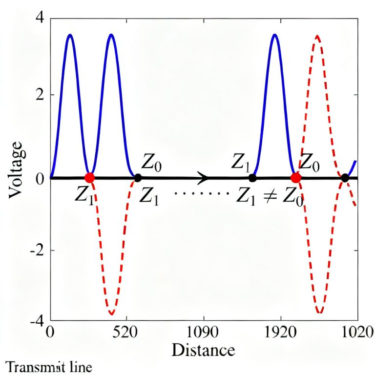
Reflection occurs when an electromagnetic wave encounters an impedance discontinuity along a transmission line. This discontinuity can be caused by changes in trace width, dielectric constant, via stubs, connectors, or terminations. The incident wave splits into a transmitted wave and a reflected wave. The ratio of reflected voltage to incident voltage defines the reflection coefficient (Γ), a complex quantity.
S11: The Return Loss Parameter in Reflection in Transmission Line Measurement Using VNA
S11 is the input reflection coefficient measured at Port 1 of a VNA. It quantifies how much of the incident signal is reflected back from the device under test (DUT). Mathematically: S11 (dB) = 20 log₁₀(|Γ|), where |Γ| = (Z_load – Z_0) / (Z_load + Z_0). Return Loss (dB) = -S11 (dB), a positive value indicating the loss of reflected power relative to incident power. A high return loss (e.g., >20 dB) indicates minimal reflection and good impedance matching, while a low return loss (e.g., <10 dB) suggests significant mismatch and potential signal integrity issues.
Why Measure S11 in High-Speed PCBs?
Reflection in Transmission Line Measurement Using VNA ensures impedance verification, troubleshooting of discontinuities like via stubs or connector transitions, and compliance with standards requiring specific return loss limits (e.g., -15 dB at 5 GHz).
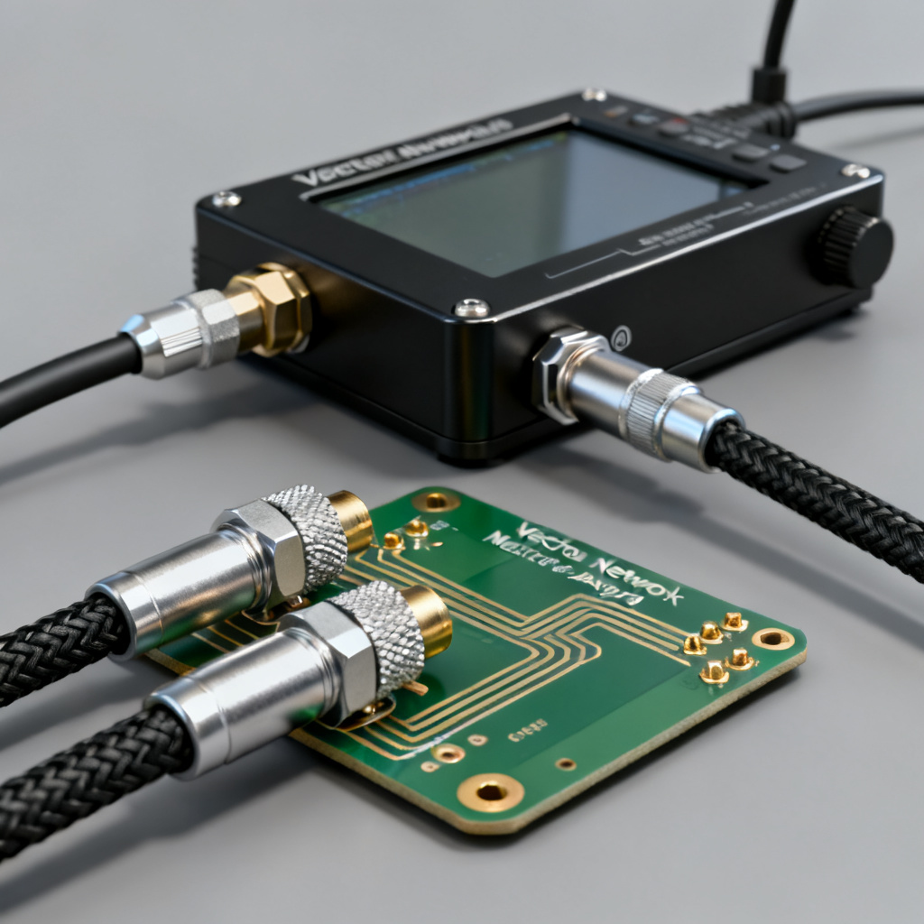
VNA Measurement Setup and Calibration for Reflection in Transmission Line Measurement Using VNA
VNA Basics for S11 Measurement
A VNA measures S-parameters by sweeping a frequency range (e.g., 10 MHz to 40 GHz) and comparing incident, reflected, and transmitted waves. For S11, only one port is needed. The VNA outputs magnitude (return loss in dB), phase (angle of reflection coefficient in degrees), and a Smith Chart (visual representation of impedance vs. frequency), enabling analysis of reflection termination behavior across frequency.
Calibration: The Key to Accuracy in Reflection in Transmission Line Measurement Using VNA
Without proper calibration, measurement errors from cables, adapters, and the VNA itself dominate. Common calibration methods: SOLT (Short-Open-Load-Through) uses known standards to correct systematic errors. For single-port S11, a SOL (Short-Open-Load) calibration at the reference plane is sufficient. TRL (Through-Reflect-Line) is more accurate for non-coaxial environments. Best Practice: Perform calibration at the exact reference plane where the DUT connects. Use low-loss, phase-stable cables and torque wrenches for connectors.
De-Embedding: Removing Fixture Effects in Reflection in Transmission Line Measurement Using VNA
Test fixtures add parasitic inductance and capacitance. De-embedding removes these effects: 2x-Thru Method measures a through line twice the length of the DUT fixture, then mathematically subtracts its S-parameters. AFR (Automated Fixture Removal) is built into modern VNAs for one-click de-embedding. Time Domain Gating uses the VNA’s time-domain transform to isolate the DUT response.
Interpreting S11 Results in Reflection in Transmission Line Measurement Using VNA
Return Loss vs. Frequency
Plot return loss (dB) vs. frequency. Key observations: Flat Response indicates consistent impedance across frequency. Resonance Dips may indicate standing waves from a specific length of mismatch. Roll-off shows gradual degradation at higher frequencies due to skin effect and dielectric loss.
Smith Chart Analysis
The Smith chart plots S11 on a polar grid of impedance. Center Point (Γ=0): Perfect 50 Ω match. Upper Half: Inductive reactance. Lower Half: Capacitive reactance. Arc Patterns: A clockwise arc indicates a transmission line length; a loop suggests a resonance.
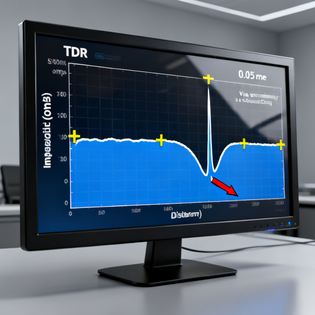
Time Domain Reflectometry (TDR) from S11
Modern VNAs convert frequency-domain S11 to time-domain using the inverse Fourier transform (IFT). This yields a TDR plot showing impedance vs. distance. Step Response reveals impedance changes along the trace. Rise Time determines spatial resolution. Gating isolates a specific section. Practical Example: A 100 mm microstrip line with a 0.5 mm via stub shows a -15 dB return loss at 15 GHz; the TDR plot reveals a 35 Ω dip at the stub location.
Sources of Measurement Error and Mitigation in Reflection in Transmission Line Measurement Using VNA
Common Errors
Cable Movement: Flexing cables after calibration changes phase. Use phase-stable cables or re-calibrate. Connector Repeatability: Poor mating adds uncertainty; use torque wrenches (e.g., 0.9 Nm for SMA). Fixture Parasitics: Un-de-embedded fixtures cause apparent mismatch; always de-embed. Temperature Drift: VNA internal drift over time; use periodic re-calibration.
Improving Accuracy
Averaging: Increase IF bandwidth averaging to reduce noise. Sweep Time: Slower sweep reduces jitter. Reference Plane Extension: Use electrical delay in VNA to shift reference plane to the DUT input.
Practical Application: High-Speed PCB Test for Reflection in Transmission Line Measurement Using VNA
Test Setup for PCB Traces
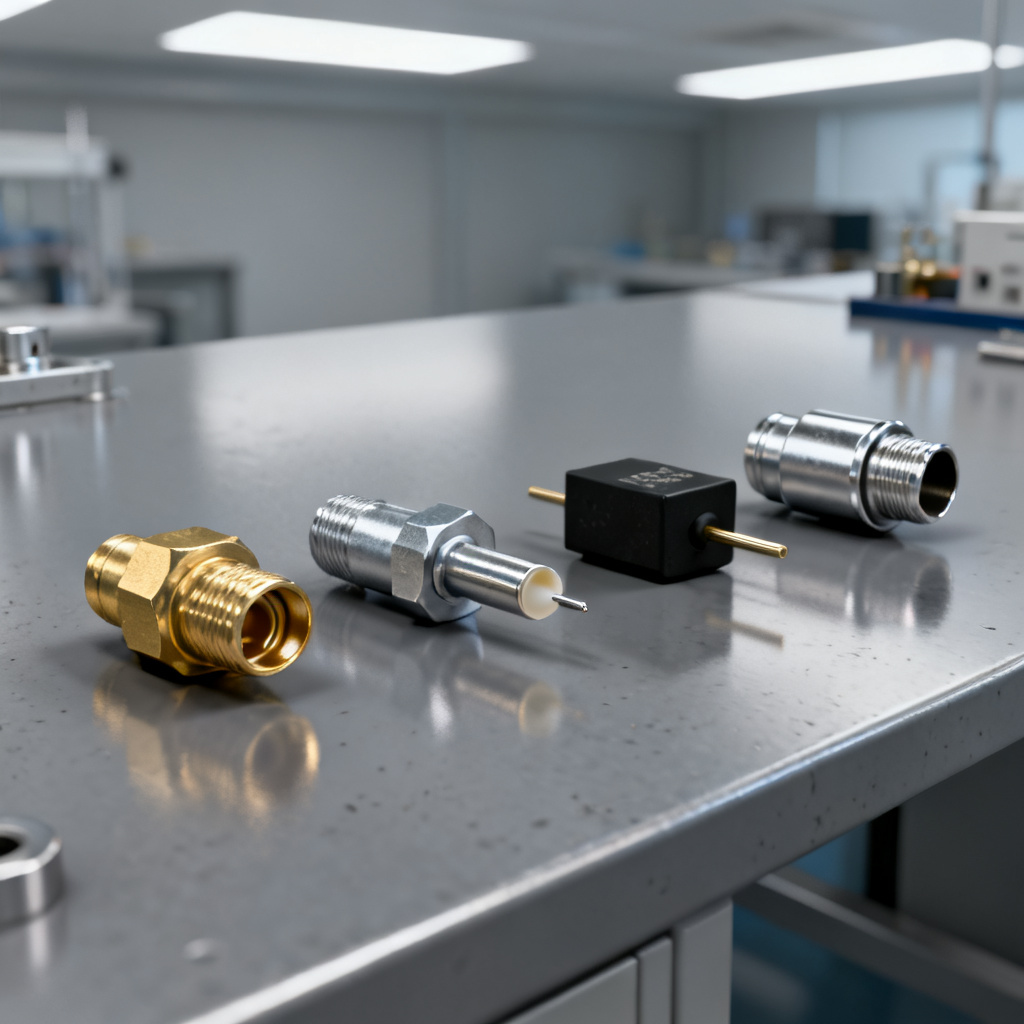
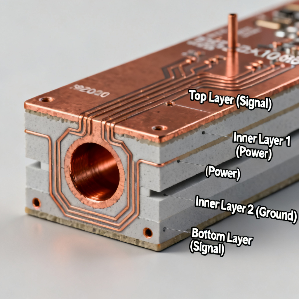
- Design Test Coupons: Include 50 Ω microstrip or stripline traces on the PCB panel. Use SMA or SMP connectors for probing.
- Calibrate VNA: Use SOLT at the connector reference plane.
- Measure S11: Sweep from low frequency to maximum operating frequency.
- De-embed: Use 2x-thru method to remove connector and launch pad effects.
- Analyze: Plot return loss and TDR. Target return loss < -20 dB for critical signals.
Case Study: Improving Return Loss in a PCIe Gen5 Trace
Problem: A PCIe Gen5 (32 Gbps) trace showed -12 dB return loss at 16 GHz, exceeding the -15 dB limit. Root Cause: TDR revealed a 45 Ω dip at a via transition due to a 0.8 mm stub. Solution: Back-drill the via to remove the stub, improving return loss to -18 dB. Verification: Re-measure S11 after back-drilling; confirm compliance.
Advanced Topics in Reflection in Transmission Line Measurement Using VNA
Differential S11 (SDD11)
For differential pairs (e.g., USB 3.0, HDMI), measure SDD11 (differential return loss). This requires a 4-port VNA or baluns. Interpretation focuses on odd-mode impedance.
Mixed-Mode S-Parameters
Modern VNAs output mixed-mode S-parameters (e.g., S_dd11, S_cc11) to analyze common-mode reflections, which cause EMI.
Correlation with Simulation
Compare measured S11 with 3D EM simulations (e.g., HFSS, CST). Discrepancies often point to manufacturing tolerances or unmodeled parasitics.
Table: Key Parameters in Reflection in Transmission Line Measurement Using VNA
| Parameter | Description | Target Value for High-Speed PCB |
|---|---|---|
| Return Loss (S11) | Reflection coefficient magnitude in dB | < -20 dB (matched lines) |
| Impedance (Z) | Characteristic impedance of trace | 50 Ω ±10% |
| Frequency Range | Measurement sweep range | 10 MHz to 40 GHz |
| TDR Resolution | Minimum distance resolvable | < 1 mm (with fast rise time) |
FAQ: Reflection in Transmission Line Measurement Using VNA
What is the difference between return loss and S11?
Return loss is the positive value of S11 (in dB). S11 is the reflection coefficient, and return loss = -S11. Both quantify reflection in transmission line measurement using VNA.
How do I calibrate a VNA for S11 measurement?
Use SOLT calibration with short, open, load standards at the reference plane. For high accuracy, use TRL calibration with a through line, reflect, and line of known delay.
What causes poor return loss in high-speed PCBs?
Common causes include via stubs, connector transitions, trace width variations, and dielectric constant changes. Reflection in transmission line measurement using VNA helps identify these discontinuities.
How can I improve S11 return loss in my PCB design?
Use back-drilling for via stubs, optimize trace geometry, select low-loss materials, and ensure proper impedance control. Regular reflection in transmission line measurement using VNA validates improvements.
Conclusion and Best Practices
Key Takeaways: S11 return loss is the primary metric for transmission line reflection in high-speed PCBs. Proper calibration and de-embedding are non-negotiable for accurate measurements. TDR from S11 provides spatial insight into impedance discontinuities. Target return loss: < -20 dB for matched lines; < -15 dB for most high-speed standards.
Recommendations for B2B PCB Designers: Include test coupons on every PCB panel. Use VNA with TDR capability. Partner with a PCB manufacturer that offers VNA-based testing and back-drilling. Document measurement conditions for reproducibility. For custom high-speed PCB fabrication with guaranteed impedance control, contact our engineering team.