Return path discontinuity amplifies crosstalk in high speed PCB design by converting clean differential signals into noisy common-mode currents. This hidden mechanism creates large current loops that radiate magnetic fields, coupling into adjacent traces far more aggressively than standard crosstalk models predict. Understanding this amplification is critical for any engineer designing 10 Gbps+ digital systems.
Physics of Return Path Discontinuity Amplifies Crosstalk
The Principle of Least Inductance
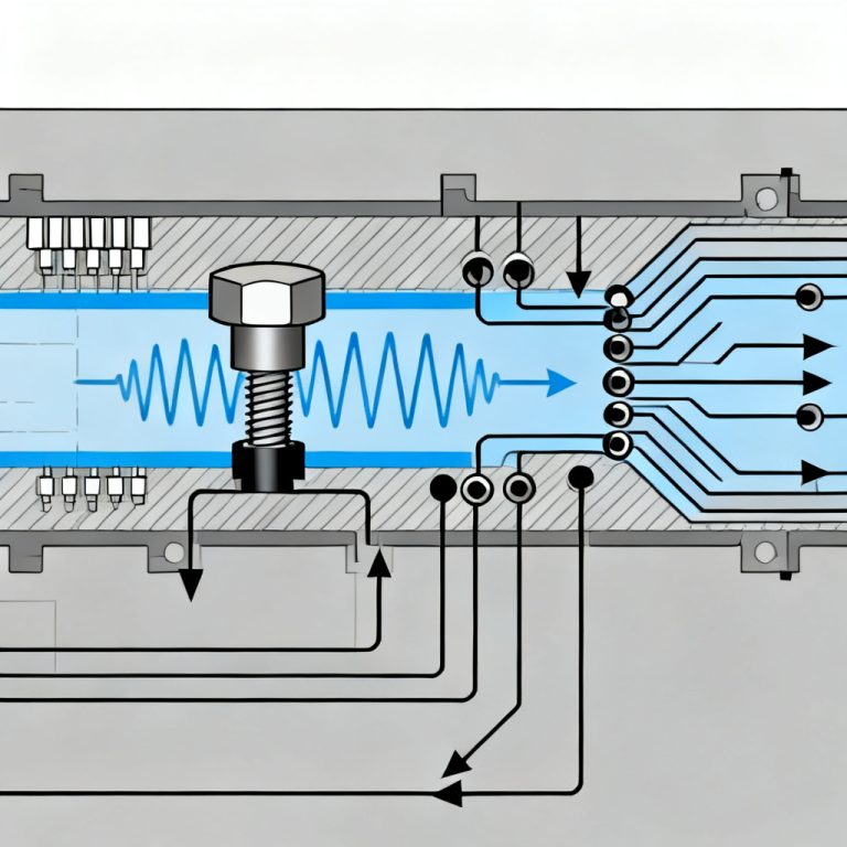
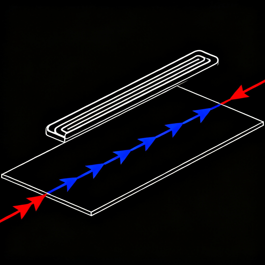
Return path discontinuity amplifies crosstalk because at high frequencies, current takes the path of least inductance. For a microstrip trace over a ground plane, the return current flows directly beneath the trace on the adjacent reference plane. This minimizes loop area and inductance. When this path is broken by a slot, split plane, or missing via stitching, the return current must find an alternative route that is longer, has higher inductance, and creates a large current loop.
The Conversion to Common-Mode Noise
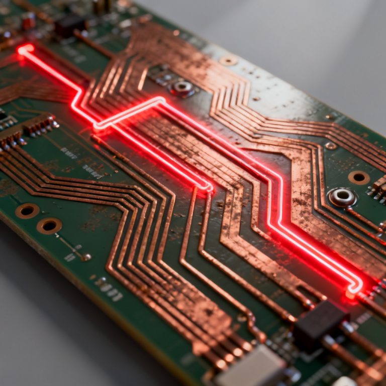
Return path discontinuity amplifies crosstalk by converting a portion of the signal energy into common-mode current. This common-mode current flows on the entire ground structure, coupling strongly into adjacent traces and cables. The result is a dramatic increase in crosstalk that is not confined to adjacent traces but can affect traces on different layers and even cables connected to the board.
Key Insight: Return path discontinuity does not create new crosstalk; it amplifies existing crosstalk by converting a clean differential signal into a noisy common-mode signal that radiates across the board.
4 Most Dangerous Scenarios Where Return Path Discontinuity Amplifies Crosstalk
Scenario 1: The Moated Island (Split Planes)
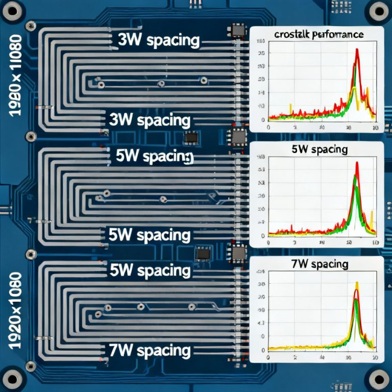
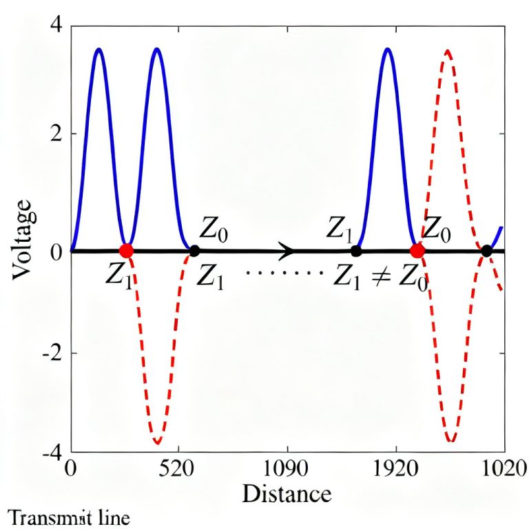
When a signal trace crosses a split in the ground plane, return path discontinuity amplifies crosstalk because the return current must travel around the split. This creates a large loop whose magnetic field couples strongly into any trace within or near the loop. Technical data shows a 100 µm gap in the plane can increase crosstalk by 10-15 dB at 1 GHz. The crosstalk is not just between the crossing trace and its neighbor but also between the two sides of the split plane.

Scenario 2: The Missing Stitching Via (Layer Transitions)
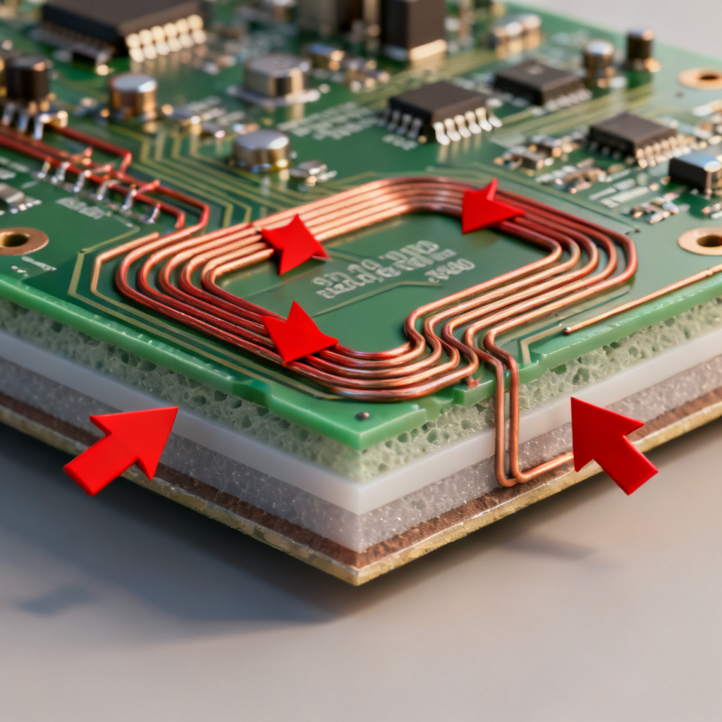
When a signal changes layers, return path discontinuity amplifies crosstalk if the two reference planes are not properly connected by a stitching via. The return current must travel from the old reference plane through the power distribution network or board edges to reach the new reference plane. This path is extremely inductive and can increase crosstalk to an adjacent victim trace by 20-30 dB compared to a properly stitched transition.
Scenario 3: The Deep Cavity (Antipad Overlap)
When a signal trace passes directly over or under a large antipad on an adjacent layer, return path discontinuity amplifies crosstalk because the return plane is effectively missing. The return current is forced to flow around the edge of the antipad, creating a localized RPD that can cause severe crosstalk to traces on the same layer near the antipad.
Scenario 4: The Long Return Path (Edge Routing and Connectors)
When a trace is routed near the board edge or transitions to a connector, return path discontinuity amplifies crosstalk because the return path is often disrupted. The return current must travel along the board edge or through the connector housing, creating a long, inductive path that couples strongly into adjacent signal-return pairs in the connector.
The Amplification Factor: Why Return Path Discontinuity Amplifies Crosstalk
Return path discontinuity amplifies crosstalk through two primary mechanisms. First, it increases mutual inductance (Lm) because the large current loop has higher self-inductance, which directly increases crosstalk voltage. Second, it converts differential-mode energy into common-mode energy, which couples into traces on different layers, through the substrate, and into cables.
Technical Detail: The simplified math shows that RPD-amplified crosstalk equals normal forward crosstalk multiplied by the ratio of the RPD loop area to the ideal loop area. This ratio can easily be 10x to 100x, meaning a 20 dB to 40 dB increase in crosstalk.
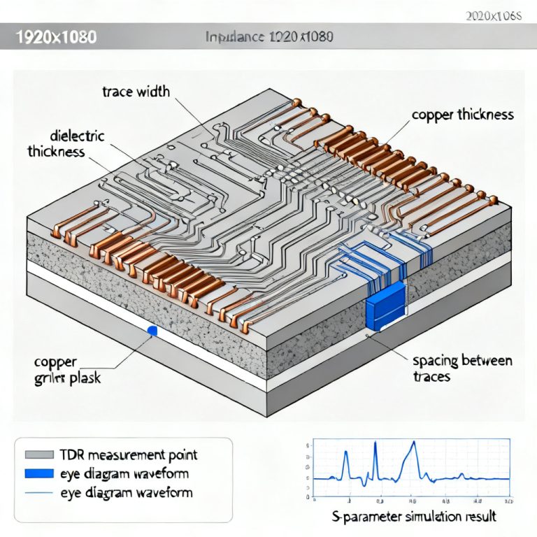
Definitive Layout Checklist to Prevent Return Path Discontinuity Amplifies Crosstalk
| Category | Action Item | Specification |
|---|---|---|
| Plane Integrity | Use a single, unbroken ground plane for all high-speed signals | Do not route across split planes |
| Via Stitching | Place a ground stitching via within 2 mm of every signal via | λ/20 rule for highest harmonic frequency |
| Spacing | Keep high-speed traces at least 10H away from board edges and slots | 10 times dielectric height |
| Connector Design | Assign every high-speed signal pin a dedicated ground pin | Use ground-filled breakout regions |
Actionable Solutions: Implement this checklist during layout to ensure return path discontinuity does not amplify crosstalk in your high speed PCB design.
Comparison: RPD-Aware Design vs. Standard Design
In standard high speed PCB design, engineers focus on trace-to-trace spacing and impedance matching. However, return path discontinuity amplifies crosstalk by 20-40 dB when these standard practices ignore return path integrity. An RPD-aware design, which includes proper via stitching, continuous reference planes, and connector ground pin assignment, reduces crosstalk to predictable levels within design margins.
Our Advantage: At [Your Company Name], we perform a mandatory Return Path Audit on every layer stack-up before routing begins. This ensures your 10 Gbps+ signals travel in a clean, low-inductance environment, free from the amplification effects of return path discontinuities.
Glossary of Key Terms
Return Path Discontinuity (RPD): A break or disruption in the ideal low-inductance path for return current in a high-speed PCB, which amplifies crosstalk by creating large current loops and converting differential-mode energy to common-mode noise.
Common-Mode Current: Current that flows in the same direction on all conductors in a system, often caused by RPD, which radiates strongly and couples into adjacent traces.
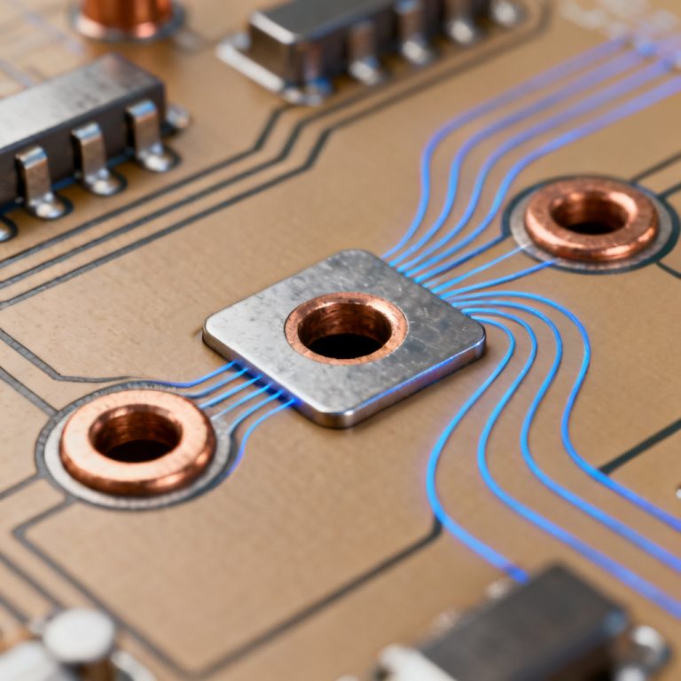
Stitching Via: A ground via placed close to a signal via during layer transitions to provide a continuous low-inductance return path.
Frequently Asked Questions
How does return path discontinuity amplify crosstalk in high speed PCB?
Return path discontinuity amplifies crosstalk by creating large current loops that increase mutual inductance and by converting differential-mode energy into common-mode noise. This can increase crosstalk by 20-40 dB compared to a design with a continuous return path.
What are the most common causes of return path discontinuity?
The most common causes are split planes, missing stitching vias during layer transitions, large antipads on adjacent layers, and routing near board edges or connectors.
How can I prevent return path discontinuity from amplifying crosstalk?
Use a single continuous ground plane, place ground stitching vias within 2 mm of every signal via, keep traces at least 10H away from board edges, and assign dedicated ground pins to every high-speed signal pin in connectors.
What is the difference between normal crosstalk and RPD-amplified crosstalk?
Normal crosstalk is limited to adjacent traces and is predictable using mutual capacitance and inductance models. RPD-amplified crosstalk can affect traces on different layers and cables, and is typically 10-100 times stronger due to the larger loop area.