In high-speed digital design, crosstalk is a critical signal integrity issue that can degrade timing margins, induce jitter, and cause false triggering. This guide focuses on how to extract Near-End and Far-End Crosstalk from S-Parameters for high speed PCB design, using frequency-domain analysis to quantify coupling. As data rates exceed 1 Gbps and rise times shrink, traditional rule-of-thumb spacing is insufficient. The most robust method to quantify crosstalk is through S-Parameter (Scattering Parameter) analysis, which is the foundation of our workflow for extracting Near-End and Far-End Crosstalk from S-Parameters.
S-Parameters provide a frequency-domain representation of a network’s electrical behavior. For crosstalk, the key parameters are:
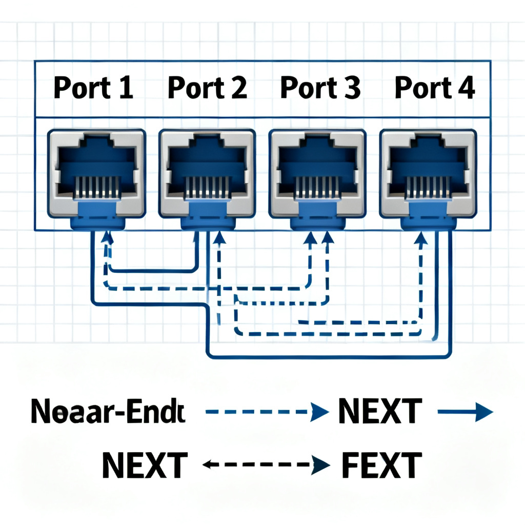
- S31 / S13: Near-End Crosstalk (NEXT) – noise coupled backward toward the aggressor source.
- S41 / S14: Far-End Crosstalk (FEXT) – noise coupled forward toward the victim load.
This pillar content explains how to extract NEXT and FEXT from S-Parameters using simulation and measurement, with a focus on practical high-speed PCB design. We synthesize the best practices from industry leaders, including Keysight, Cadence, and IEEE standards, ensuring you can apply these techniques to your next design.
Understanding S-Parameters and Crosstalk Mechanisms for High Speed PCB
The Basics of S-Parameters
S-Parameters describe how RF energy propagates through a multi-port network. For a 4-port system (2 transmission lines), the S-matrix is:
[b] = [S] * [a]
Where a is the incident wave and b is the reflected wave. The ports are typically defined as:
- Port 1: Input of the aggressor line.
- Port 2: Output of the aggressor line.
- Port 3: Near-end of the victim line (same side as Port 1).
- Port 4: Far-end of the victim line (same side as Port 2).
Key S-Parameters for Crosstalk:
- S11: Input return loss (aggressor).
- S21: Insertion loss (aggressor to aggressor output).
- S31: NEXT – power coupled from Port 1 to Port 3.
- S41: FEXT – power coupled from Port 1 to Port 4.
NEXT vs. FEXT: Physical Origins
Near-End Crosstalk (NEXT): Occurs when the forward-traveling wave on the aggressor line induces a backward-traveling wave on the victim line. This backward wave is due to both capacitive and inductive coupling. NEXT is strongest when the aggressor and victim are close together at the driver end. It is typically constant with line length (for long lines) because the backward wave integrates over the entire line.
Far-End Crosstalk (FEXT): Occurs when the forward-traveling wave on the aggressor induces a forward-traveling wave on the victim. FEXT results from the difference between the inductive and capacitive coupling coefficients (i.e., the modal velocity mismatch). In homogeneous media (e.g., stripline), FEXT is theoretically zero. In microstrip, it is significant and increases with line length and frequency.
Why Extract from S-Parameters? S-Parameters capture all these complex interactions in a single frequency-domain sweep, including reflections, losses, and coupling. This allows SI engineers to simulate time-domain crosstalk via Inverse Fast Fourier Transform (IFFT) or to directly set crosstalk budgets in frequency domain.
Step-by-Step Extraction Methodology for Near-End and Far-End Crosstalk from S-Parameters
Setup for Extracting Near-End and Far-End Crosstalk from S-Parameters: Simulation or Measurement
Simulation (Using EM Solvers):
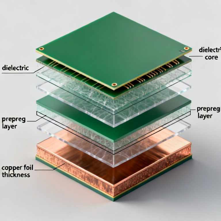
- Define the Geometry: Create a 2D or 3D model of your PCB stackup. Include trace width, spacing, dielectric thickness, and material properties (Dk, Df). Use a 4-port configuration.
- Port Definition: Assign ports at the ends of each trace. Ensure ports are de-embedded to the reference plane (e.g., using a TDR or calibration kit in simulation).
- Frequency Sweep: Sweep from DC to at least 5x the highest harmonic of your signal (e.g., for 10 Gbps, sweep to 50 GHz).
- Extract S-Parameters: Export the Touchstone (.s4p) file.
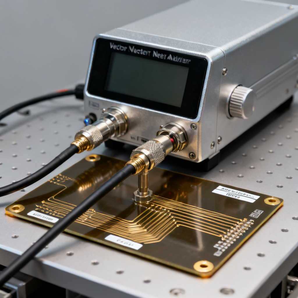
Measurement (Using VNA):
- Calibration: Perform a full 2-port or 4-port calibration (SOLT or TRL) to remove cable and fixture effects.
- DUT Connection: Connect your PCB test coupon (e.g., a pair of coupled microstrip lines).
- Acquire Data: Measure S11, S21, S31, S41 across the desired frequency range.
- Post-Processing: Apply time-domain gating to remove connector reflections.
Direct Extraction from S-Parameters
Extracting NEXT (S31):
- For a single-ended aggressor and victim, NEXT in dB is directly:
NEXT(dB) = 20 * log10(|S31|) - To convert to voltage or power crosstalk coefficient:
NEXT_coefficient = |S31|
Extracting FEXT (S41):
- Similarly:
FEXT(dB) = 20 * log10(|S41|) - Note: S41 is often much smaller than S31 at low frequencies but grows with frequency.
Critical Considerations:
- Port Impedance: S-Parameters are typically referenced to 50 ohms. If your system uses a different impedance (e.g., 100 ohms differential), you must renormalize the S-parameters.
- Phase Information: For time-domain reconstruction, you need the full complex S-parameters (magnitude and phase). Most simulation tools output this automatically.
- De-embedding: Ensure that the S-parameters represent only the PCB trace, not the connectors or launch pads. Use de-embedding techniques (e.g., 2x-thru or TRL calibration) to isolate the DUT.
Converting to Time-Domain (TDR/TDT)
To see crosstalk as a waveform (e.g., for eye diagram analysis), convert S-parameters to time-domain:
- IFFT (Inverse Fast Fourier Transform): Apply an IFFT to S31 and S41. This yields the impulse response of the crosstalk channel.
- Convolution: Convolve the impulse response with your digital signal (e.g., PRBS pattern) to get the time-domain crosstalk waveform.
- Peak Crosstalk: Measure the peak-to-peak or RMS crosstalk voltage from the waveform.
Tools:
- Keysight ADS: Use the
S-Parameter to Time Domainutility. - Cadence Sigrity: Use the
Crosstalk Analysisworkflow. - Python/Scipy: Use
scipy.signal.freqzandnumpy.fftfor custom scripts.
Advanced Interpretation and Practical Tips for High Speed PCB Crosstalk Analysis
Frequency vs. Time-Domain Crosstalk
- Frequency Domain (S-Parameters): Ideal for understanding resonant peaks, bandwidth limitations, and coupling mechanisms. For example, a resonance in S31 indicates a standing wave due to impedance mismatch.
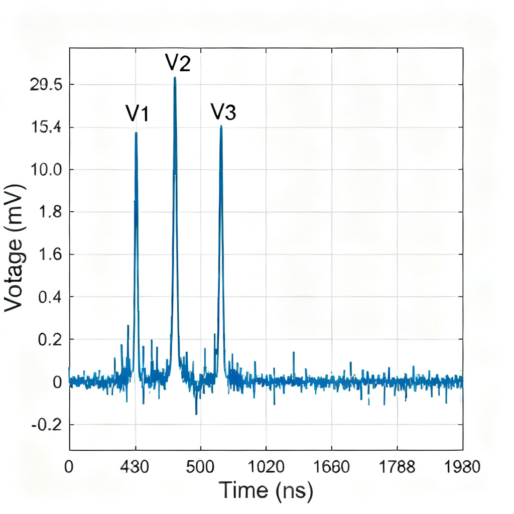
- Time Domain (TDR/TDT): Essential for digital designers. It shows the exact timing of crosstalk events (e.g., near-end crosstalk appears immediately after the aggressor edge; far-end crosstalk appears after a propagation delay).
Rule of Thumb:
- Use S-parameters for design validation and compliance testing (e.g., IEEE 802.3).
- Use time-domain crosstalk for system-level margins and eye diagram analysis.
Common Pitfalls and How to Avoid Them
- Ignoring Mode Conversion: In differential pairs, NEXT and FEXT are defined differently. For differential aggressors, you need mixed-mode S-parameters (SDD31, SCC31, etc.). Always use differential S-parameters for differential designs.
- Incorrect Port Reference: If your VNA calibration is poor, or your simulation ports are not de-embedded, S31 and S41 will include connector and launch effects. Always validate with a known standard.
- Assuming Linear Scaling: Crosstalk does not always scale linearly with length. For NEXT, it saturates after a critical length (typically when the round-trip delay exceeds the rise time). For FEXT, it grows linearly with length in microstrip.
- Frequency Bandwidth: Ensure your S-parameter sweep covers frequencies up to the Nyquist rate (or higher). Missing high-frequency content will underestimate crosstalk.
Using S-Parameters for Design Optimization
- Spacing Analysis: Simulate multiple geometries (e.g., 2x, 3x, 5x trace width spacing) and extract S31/S41. Plot the crosstalk vs. spacing curves to find the minimum spacing that meets your budget (e.g., -40 dB at 10 GHz).
- Shielding Effectiveness: Compare S31 for a trace with and without a ground guard trace. A guard trace can reduce NEXT by 10-20 dB if properly stitched with vias.
- Material Impact: Use S-parameters to evaluate how different dielectrics (e.g., FR4 vs. low-loss materials) affect FEXT. Low-loss materials reduce attenuation but may increase modal velocity mismatch.
Case Study – Extracting Crosstalk from a High-Speed PCB
Scenario: You are designing a 28 Gbps NRZ link on a 10-layer PCB. Aggressor and victim are 5 mil wide microstrip traces on the top layer, spaced 5 mil apart, with a 4 mil prepreg. You want to ensure NEXT < -35 dB and FEXT < -40 dB at 14 GHz (Nyquist).
Step 1: Simulate S-Parameters Use Ansys HFSS or Keysight Momentum. Set up a 4-port model with 1-inch traces. Sweep from 100 MHz to 50 GHz.
Step 2: Extract S31 and S41
- S31 at 14 GHz: -32 dB (exceeds budget).
- S41 at 14 GHz: -38 dB (within budget).
Step 3: Time-Domain Conversion
- NEXT impulse response shows a peak of 0.12 V (for a 1 V aggressor).
- FEXT impulse response shows a peak of 0.05 V.
Step 4: Optimization Increase spacing to 10 mil. Re-simulate:
- S31 at 14 GHz: -40 dB.
- S41 at 14 GHz: -45 dB.
- NEXT peak drops to 0.04 V.
Conclusion: Spacing must be at least 10 mil to meet the budget. This is validated by S-parameter extraction.
Frequently Asked Questions about Extracting Near-End and Far-End Crosstalk from S-Parameters
Can I extract NEXT and FEXT from a 2-port measurement?
No. You need a 4-port measurement (or a 2-port with a switch matrix) to capture all coupling paths for extracting Near-End and Far-End Crosstalk from S-Parameters.
What is the difference between S31 and S13?
In a reciprocal network, S31 = S13. They represent the same coupling path but with the source and load swapped. For crosstalk extraction, S31 is the standard.
How do I convert S-parameter crosstalk to a crosstalk coefficient (Kb, Kf)?
- NEXT coefficient (Kb) = |S31| / (1 – |S11|^2) (approximately, for weak coupling).
- FEXT coefficient (Kf) = |S41| / (1 – |S21|^2).
This accounts for losses and mismatches.
My S-parameters show negative dB values for crosstalk. Is that correct?
Yes. Crosstalk is a loss mechanism, so it is always less than 0 dB. -40 dB means 1% voltage coupling.
Do I need to consider phase for crosstalk extraction?
For magnitude-only budgets (e.g., -40 dB at 14 GHz), phase is not needed. For time-domain waveform reconstruction, phase is critical.
Conclusion: Integrating S-Parameter Crosstalk Analysis into Your High Speed PCB Design Flow
Conclusion: Integrating S-Parameter Crosstalk Analysis into Your High Speed PCB Design Flow.
Extracting Near-End and Far-End Crosstalk from S-Parameters is not just a theoretical exercise—it is a practical necessity for high-speed PCB design. By following the methodology outlined here—setting up accurate simulations or measurements, directly reading S31 and S41, converting to time-domain when needed, and iterating on geometry—you can ensure your design meets stringent signal integrity requirements. This is why mastering how to extract Near-End and Far-End Crosstalk from S-Parameters is a must-have skill for any SI engineer working on 10Gbps+ links.
By following the methodology outlined here—setting up accurate simulations or measurements, directly reading S31 and S41, converting to time-domain when needed, and iterating on geometry—you can ensure your design meets stringent signal integrity requirements.
At [Your Company Name], we specialize in manufacturing high-speed PCBs optimized for minimal crosstalk. Our design-for-manufacturing (DFM) team can simulate your stackup and provide pre-layout S-parameter analysis to guarantee first-pass success. Contact us today to discuss your next 28 Gbps+ project.
Key Terminology for High Speed PCB Crosstalk Analysis
| Term | Definition Related to High Speed PCB Crosstalk |
|---|---|
| Signal Integrity (SI) | Ensuring that electrical signals are transmitted without distortion, directly impacted by crosstalk. |
| Impedance Control | Maintaining consistent characteristic impedance (e.g., 50 ohms) to minimize reflections and crosstalk. |
| Differential Pair | Two traces carrying opposite signals; common-mode noise and crosstalk are analyzed via mixed-mode S-parameters. |
| De-embedding | Removing fixture effects from measurements to isolate the PCB trace’s S-parameters. |
| Touchstone File | Standard file format (.s4p) for storing frequency-domain S-parameter data used in crosstalk extraction. |
Comparison: Our High Speed PCB Manufacturing vs. Generic Fabricators
| Feature | Our High Speed PCB Service | Generic Fabricator |
|---|---|---|
| Crosstalk Analysis Support | Pre-layout S-parameter simulation and DFM feedback | Limited to basic spacing rules |
| Impedance Control Accuracy | ±5% tolerance, validated with TDR | ±10% typical |
| Material Options | Low-loss laminates (e.g., Megtron 6, Rogers) | Standard FR4 only |
| Testing Capabilities | 4-port VNA measurement and time-domain analysis | 2-port TDR only |