To master high-speed PCB design, you must learn Polar Si9000 for Crosstalk and know how to use this tool to estimate crosstalk in high speed PCB before routing. This pre-layout estimation enables you to define critical design rules—trace spacing, dielectric thickness, and stackup geometry—that guarantee your high-speed signals remain clean. This guide synthesizes the most authoritative knowledge from leading PCB design resources to give you a step-by-step, no-nonsense workflow for using Polar Si9000 for Crosstalk to predict and mitigate crosstalk.

1. Fundamentals of Crosstalk in High Speed PCB
Before diving into the software, you must understand the physics Polar Si9000 is modeling. Crosstalk in high speed PCB is driven by two coupling mechanisms:
- Capacitive (Electric) Coupling: Determined by the mutual capacitance between traces. It is proportional to the overlap area of the traces and the dielectric constant of the material. It increases as the traces get closer and as the dielectric gets thinner.
- Inductive (Magnetic) Coupling: Determined by the mutual inductance between the signal loop and the return path. It is dominant in high-speed designs because the rate of change of current (di/dt) is high. It is heavily influenced by the height of the trace above the reference plane.
Key Metrics in Polar Si9000 for Crosstalk Analysis
- Mutual Inductance (Lm): Measured in nH per unit length. Directly correlates to inductive crosstalk.
- Mutual Capacitance (Cm): Measured in pF per unit length. Directly correlates to capacitive crosstalk.
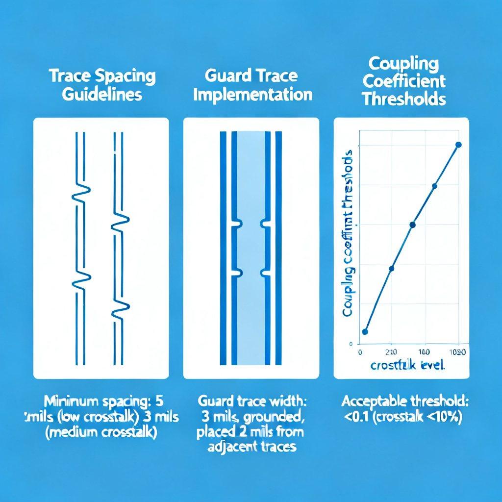
- Coupling Coefficient (K): A dimensionless number (0 to 1) describing the fraction of magnetic flux shared between two traces. A K value above 0.1 is generally considered high-risk for high-speed designs.
The critical rule for crosstalk in high speed PCB is: Crosstalk is a near-field phenomenon. It drops off dramatically with increased trace separation. In most standard FR4 stackups, the crosstalk is negligible when the center-to-center spacing is greater than 3 to 5 times the dielectric height (H). Polar Si9000 will help you find this exact “sweet spot.”
2. Setting Up Your Stackup in Polar Si9000 for Crosstalk Estimation
The first step in how to use Polar Si9000 to estimate crosstalk in high speed PCB is defining your PCB’s physical geometry. Polar Si9000’s power lies in its ability to model complex, real-world stackups. Do not skip this step—inaccurate geometry leads to useless crosstalk estimates.
Step 2.1: Choose the Correct Field Solver Type
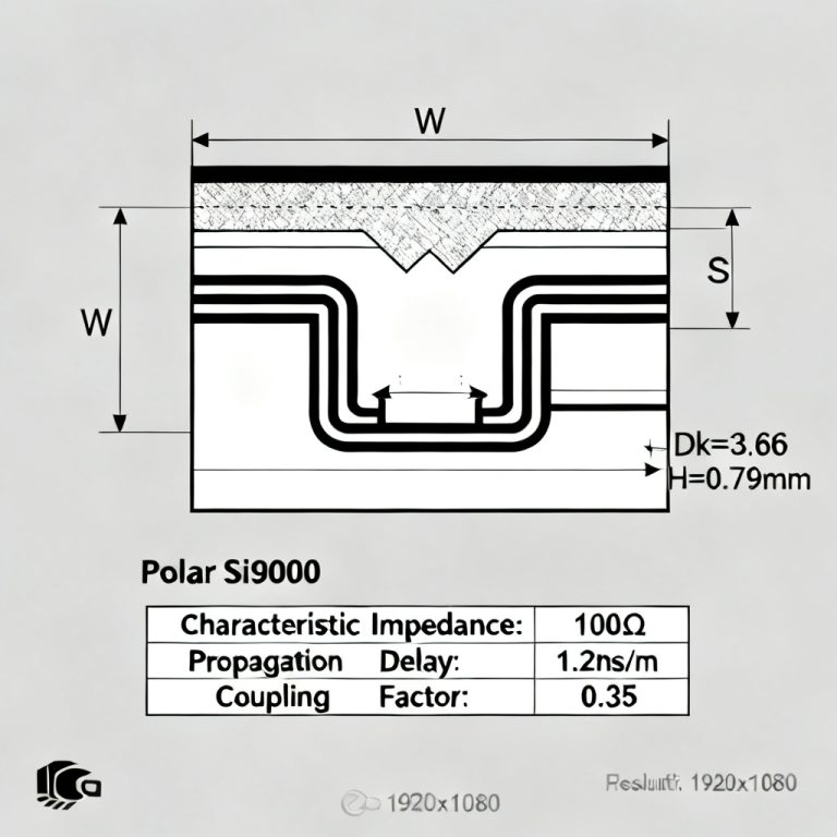
- For crosstalk, you will primarily use the 2D Boundary Element Field Solver. This is the standard for analyzing coupled transmission lines.
- For very high frequencies (above 20 GHz) or when dealing with extremely thin dielectrics (e.g., < 50 microns), consider the 2D FEM (Finite Element Method) solver for higher accuracy, though it is computationally slower.
Step 2.2: Define the Layer Stackup
Navigate to the “Stackup” or “Substrate” tab. Input your exact layer structure from your PCB manufacturer’s validated stackup. You must enter:
- Dielectric Material: e.g., FR4 (standard), Rogers 4350B (high-frequency), or Isola 370HR. Enter the exact dielectric constant (Dk) and loss tangent (Df) at your target frequency (e.g., 1 GHz, 10 GHz).
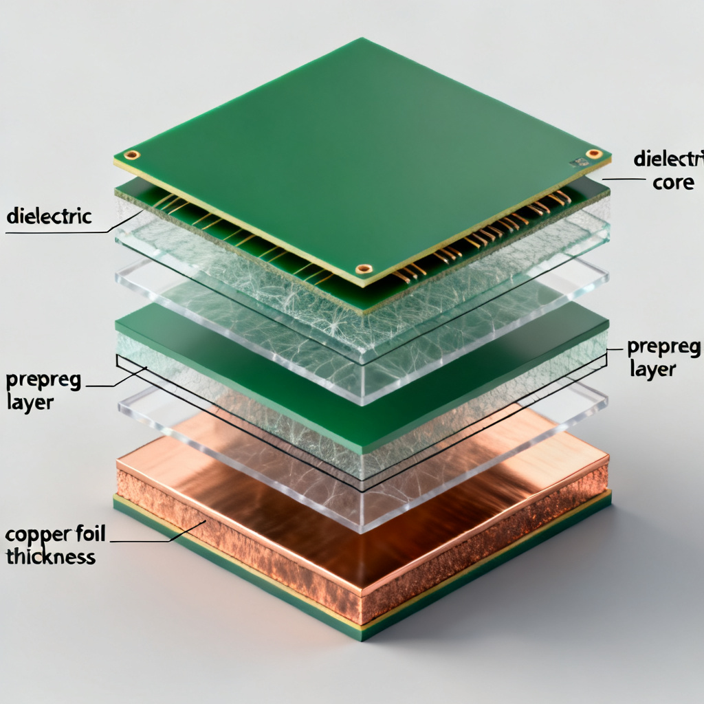
- Core and Prepreg Thickness: Enter the finished thickness of each core and prepreg layer. Remember that prepreg thickness can vary depending on resin content and copper weight.
- Copper Weight: Enter the copper thickness (e.g., 0.5 oz, 1 oz, 2 oz). This affects the trace geometry and thus the crosstalk.
Step 2.3: Define the Trace Geometry
For a crosstalk analysis, you need to model at least two traces. Select the “Coupled Microstrip” or “Coupled Stripline” structure, depending on your signal layer.
- Trace Width (W): Enter your target impedance-controlled width (e.g., 5 mils for 50 ohms).
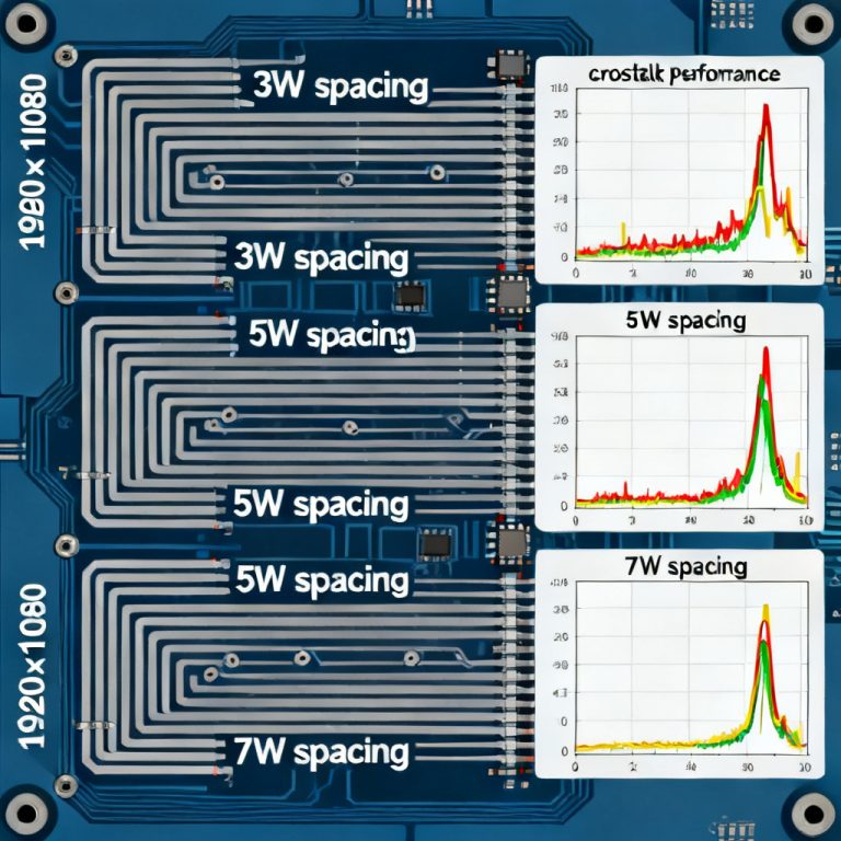
- Trace Spacing (S): This is the variable you will sweep. Start with a minimum spacing (e.g., 5 mils) and increase it.
- Trace Thickness (T): Enter the copper thickness.
- Reference Plane: Ensure the top and bottom (for stripline) reference planes are correctly defined as “Plane” (solid copper pour).
Expert Tip: Always model the worst-case scenario. If your design has a mix of 50-ohm and 100-ohm differential traces, model the 50-ohm single-ended traces first, as they often have tighter coupling to the reference plane, leading to higher inductive crosstalk.
3. Running the Crosstalk Simulation in Polar Si9000
Now that your stackup is defined, you will run the simulation to extract the coupling parameters. This is the core of how to use Polar Si9000 to estimate crosstalk in high speed PCB.
Step 3.1: Launch the Crosstalk Module
In Polar Si9000, go to the “Calculation” menu and select “Crosstalk Analysis” or “Mutual Inductance/Capacitance”. The exact name depends on your version.
Step 3.2: Configure the Simulation
- Frequency: Set a single frequency for the analysis. A good starting point is the fundamental frequency of your fastest signal (e.g., 1 GHz for a 1 Gbps signal, or the 3rd harmonic for edge-rate analysis). Polar’s results are relatively flat over a wide frequency range for typical FR4, so a single frequency is often sufficient for pre-layout estimation.
- Length: Enter a unit length (e.g., 1 inch or 10 mm). The results will be per-unit-length.
- Units: Ensure consistency (mils, mm, inches).
Step 3.3: Run the Simulation and Interpret Results
Click “Calculate.” The tool will output a comprehensive report. Focus on these key parameters for crosstalk in high speed PCB:
- Mutual Inductance (Lm): This is the most critical number for high-speed crosstalk. A typical value for a tightly coupled pair (5 mil spacing, 5 mil trace width) on a standard 4-layer board might be 0.5 to 1.0 nH/inch. Anything above 0.3 nH/inch for a 1-inch parallel run on a 1 GHz signal warrants careful attention.
- Mutual Capacitance (Cm): This is less dominant at high speeds but still important. Typical values range from 0.1 to 0.5 pF/inch.
- Coupling Coefficient (K): Calculated as
K = Lm / sqrt(L1 * L2), where L1 and L2 are the self-inductances of the two traces. A K value of 0.1 or higher is a red flag. It indicates that 10% or more of the magnetic field from one trace is coupling into the other. - Odd and Even Mode Impedances: These are derived from the coupling. If the odd-mode impedance (Zodd) is significantly lower than the even-mode impedance (Zeven), you have strong coupling. The difference (Zeven – Zodd) is a direct measure of crosstalk strength.
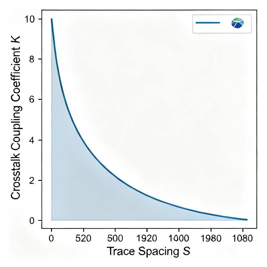
Pro Tip: Use the “Sweep feature” in Polar Si9000. Set the trace spacing (S) as the variable, and sweep it from the minimum allowed by your manufacturer (e.g., 4 mils) to a large value (e.g., 20 mils). Plot the resulting Lm, Cm, and K values. You will see a steep drop-off in crosstalk as spacing increases. The “knee” of this curve (where the drop-off slows) is your optimal minimum spacing.
4. Setting Pre-Layout Design Rules from the Simulation
The ultimate goal of how to use Polar Si9000 to estimate crosstalk in high speed PCB is not just to get numbers, but to convert those numbers into actionable PCB layout rules. Here is how to translate your simulation results:
Rule 1: Determine Minimum Trace Spacing (The “3H” Rule, Refined)
The classic “3H” rule (spacing = 3x the dielectric height) is a starting point, but it is often too conservative or too aggressive. Use Polar Si9000 to find the exact spacing for your specific stackup.
- Action: From your sweep data, find the spacing (S) where the coupling coefficient (K) drops below 0.05 (for high-speed digital) or 0.02 (for RF/analog). That is your new minimum spacing rule.
- Example: If your dielectric height (H) is 5 mils, and your sweep shows K=0.05 at S=15 mils, then your rule is S >= 15 mils (3H). But if K=0.05 at S=12 mils, your rule is S >= 12 mils (2.4H). You just saved 3 mils of routing channel space.
Rule 2: Define Critical Parallel Run Lengths
Crosstalk is a cumulative effect. The longer two traces run parallel, the more crosstalk builds up.
- Action: Use the formula:
Crosstalk Voltage (Vxt) = (Lm * di/dt) + (Cm * dv/dt). You can simplify this by using the coupling coefficient. A common rule of thumb is that for a 1-inch parallel run with K=0.1, the near-end crosstalk (NEXT) is approximately 10% of the signal voltage. - Rule: If your simulation shows K=0.08 at S=10 mils, then for a 5-inch parallel run, the total NEXT could be 40% (5 * 8%). This is unacceptable. Therefore, set a rule: “Maximum parallel run length at S=10 mils is 1.5 inches.” Beyond that, you must increase spacing or use guard traces.
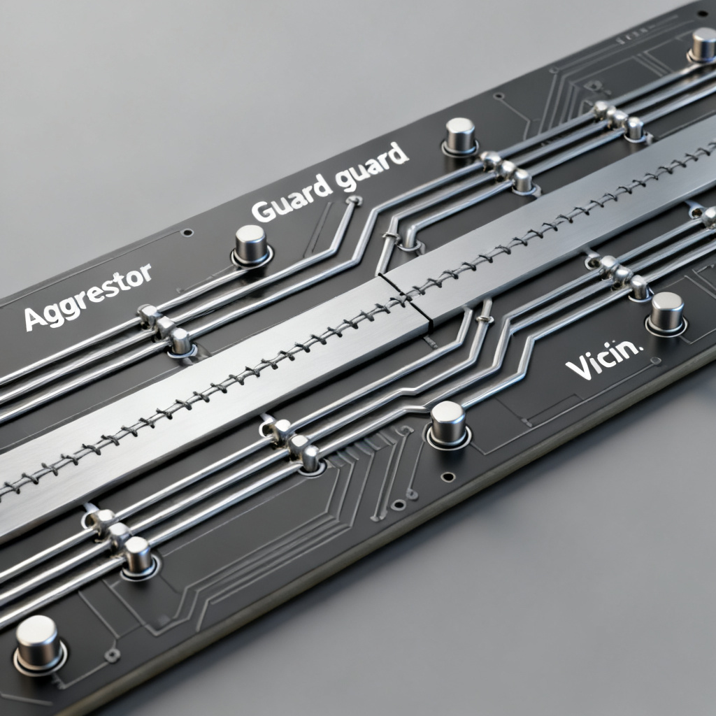
Rule 3: Implement Guard Traces (and How to Size Them)
A guard trace (a grounded copper trace placed between aggressor and victim) can dramatically reduce crosstalk in high speed PCB, but only if designed correctly.
- Action: In Polar Si9000, model a three-trace structure: Aggressor – Guard Trace – Victim. Set the guard trace width to be at least 2x the signal trace width.
- Simulation: Run the crosstalk analysis with the guard trace grounded (connected to the reference plane via vias at both ends). You will see a 50-80% reduction in Lm and Cm compared to the two-trace model.
- Rule: “If spacing cannot be increased beyond 1.5H, use a grounded guard trace with width = 2W and via stitching at every 1/10th of the signal wavelength.”
5. Advanced Techniques and Common Pitfalls
Advanced Technique: Modeling Skew and Differential Pairs
For differential pairs, crosstalk is less of a problem within the pair (it is designed to be coupled). The real issue is crosstalk between differential pairs. In Polar Si9000, model a “Coupled Differential Pair” structure. The key metric is the differential-to-common mode conversion. A high value indicates that crosstalk from an external aggressor is converting your clean differential signal into unwanted common-mode noise.
- Action: Simulate two differential pairs running parallel. Sweep the spacing between the pairs. The goal is to keep the differential impedance of each pair stable and minimize the common-mode noise induced by the adjacent pair.
Common Pitfall 1: Ignoring the Return Path
Crosstalk is fundamentally a loop phenomenon. If your reference plane is split or has a slot, the return current for the aggressor trace must take a longer path. This increases the loop area and dramatically increases inductive crosstalk.
- Rule: Never route high-speed traces over a split plane (e.g., an analog/digital split). Polar Si9000 assumes a solid, continuous reference plane. If your board has splits, your simulation results are invalid.
Common Pitfall 2: Using the Wrong Dielectric Constant
Using a generic Dk of 4.2 for FR4 is not accurate at high frequencies. At 1 GHz, the Dk of standard FR4 can drop to 4.0 or lower. At 10 GHz, it can be 3.8. Using a higher Dk in Polar Si9000 will make the traces appear wider (for a given impedance), which artificially increases the mutual capacitance and overestimates crosstalk.
- Action: Obtain the frequency-dependent Dk from your laminate supplier. Use the value at your signal’s fundamental frequency.
Common Pitfall 3: Forgetting about Via Stitching
Guard traces are useless without proper via stitching. A floating guard trace acts as a secondary aggressor.
- Rule: When using a guard trace, place vias at both ends and at every 1/10th of the signal wavelength along its length. For a 1 GHz signal (wavelength ~6 inches in FR4), this means vias every 0.6 inches.
6. Comparison: Polar Si9000 vs. Other Crosstalk Estimation Methods
| Method | Crosstalk Accuracy for High Speed PCB | Ease of Pre-Layout Use | Cost |
|---|---|---|---|
| Polar Si9000 | High (2D field solver, validated by fabricators) | Excellent (standalone, no 3D model needed) | Moderate (license required) |
| Ansys Q2D Extractor | Very High (2D/3D hybrid) | Moderate (requires integration) | High (enterprise license) |
| Manual Calculation (Formulas) | Low (approximations only) | Poor (time-consuming, error-prone) | Free |
7. Industry Terminology for Crosstalk in High Speed PCB
- NEXT (Near-End Crosstalk): Noise measured at the near end of the victim trace, traveling in the opposite direction of the aggressor signal.
- FEXT (Far-End Crosstalk): Noise measured at the far end of the victim trace, traveling in the same direction as the aggressor signal.
- Mutual Inductance (Lm): The magnetic coupling between two traces, measured in nH per unit length.
- Coupling Coefficient (K): A ratio of mutual inductance to self-inductance, indicating the strength of magnetic coupling.
- 3W Rule: A design guideline stating that trace spacing should be at least three times the trace width to minimize crosstalk.
- Guard Trace: A grounded copper trace placed between signal traces to reduce electromagnetic coupling.
8. Frequently Asked Questions about Polar Si9000 and Crosstalk
Q1: What is the most important parameter to check in Polar Si9000 for crosstalk in high speed PCB?
A: The Coupling Coefficient (K) is the most important single parameter. A K value above 0.1 indicates significant magnetic coupling and potential signal integrity issues.
Q2: Can I use Polar Si9000 to estimate crosstalk for differential pairs?
A: Yes. Use the “Coupled Differential Pair” structure in Polar Si9000. Focus on the differential-to-common mode conversion to assess inter-pair crosstalk.
Q3: How does trace spacing affect crosstalk in high speed PCB?
A: Increasing trace spacing reduces both mutual inductance and mutual capacitance exponentially. The “3W Rule” (spacing = 3x trace width) is a common starting point, but Polar Si9000 allows you to optimize spacing for your specific stackup.
Q4: Is Polar Si9000 accurate for estimating crosstalk at frequencies above 10 GHz?
A: For frequencies above 10 GHz, consider using the 2D FEM solver in Polar Si9000 for higher accuracy. The standard boundary element solver may have limitations at very high frequencies.
Q5: What is the role of the return path in crosstalk estimation?
A: A continuous, solid reference plane minimizes the loop area and reduces inductive crosstalk. Any discontinuity in the return path significantly increases crosstalk. Polar Si9000 assumes a solid reference plane, so ensure your PCB design maintains this integrity.