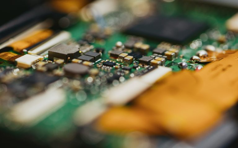
High-speed PCB manufacturing is the core hardware foundation of modern high-bandwidth electronics, including servers, data center hardware, 5G communication devices, high-performance computing, and millimeter-wave systems. Unlike conventional standard PCBs, high-speed PCB manufacturing requires ultra-precise process control, low-loss material matching, advanced via technologies like back drilling, and strict impedance stability throughout fabrication.
1. Introduction: What Is High-Speed PCB Manufacturing
High-speed PCB manufacturing produces boards engineered to support high-frequency, high-data-rate transmission ranging from 3Gbps basic signals to 112G PAM4 ultra-fast communication infrastructures. While standard PCBs focus on basic electrical connectivity, high-speed PCB manufacturing focuses on signal integrity, low dielectric loss, stable characteristic impedance, reduced crosstalk, and long-term reliability.
Core Differences from Ordinary PCB Production
Traditional circuit boards allow large process tolerances that cannot meet high-frequency demands. The key distinctions below define the entire philosophy of high-speed PCB manufacturing:
| Characteristic | Standard PCB | High-Speed PCB |
|---|---|---|
| Impedance tolerance | ±15% | ±10% (standard), ±7% or ±5% (tight) |
| Line width accuracy | ±20% | ±10% or better |
| Testing | Continuity & isolation | TDR + VNA + Four-wire Kelvin |
| Special processes | Optional | back drilling, sequential lamination, HDI process |
| Material selection | Standard FR-4 | Low-loss, mid-loss, or ultra-low-loss laminates |
Why high-speed PCB manufacturing needs stricter control:
- Tighter impedance tolerance directly affects signal reflection and timing
- Ultra-high dimensional precision prevents crosstalk and EMI
- Advanced via techniques eliminate stub resonance
- Low-loss materials minimize high-frequency attenuation
- Multi-level testing captures defects before field deployment
2. Overall Process Flow for High-Speed PCB Manufacturing
High-speed PCB manufacturing follows a rigid, step-by-step workflow. Each procedure in high-speed PCB manufacturing is interconnected, ensuring stable multilayer structure, uniform dielectric thickness, and consistent electrical performance.
Complete Production Sequence
Raw Material Cutting → Inner Layer Dry Film Lamination & Exposure → Precision Chemical Etching → AOI Defect Inspection → Copper Surface Brownization → Multilayer High-Pressure Lamination → Mechanical & Laser Drilling → Desmear Residue Removal → Electroless Copper Plating → Electroplating Copper Thickening → Outer Layer Imaging & Etching → Secondary AOI Inspection → LPI Solder Mask Coating & Development → Custom Surface Finish → Board Routing & Profiling → Comprehensive Electrical Testing → Final Dimension & Visual Inspection → Vacuum Packaging & Global Delivery
Why Every Step Matters
Even small fluctuations in lamination temperature, etching speed, or drilling depth can trigger impedance drift and degraded high-frequency performance, making full-process standardization essential for successful high-speed PCB manufacturing.
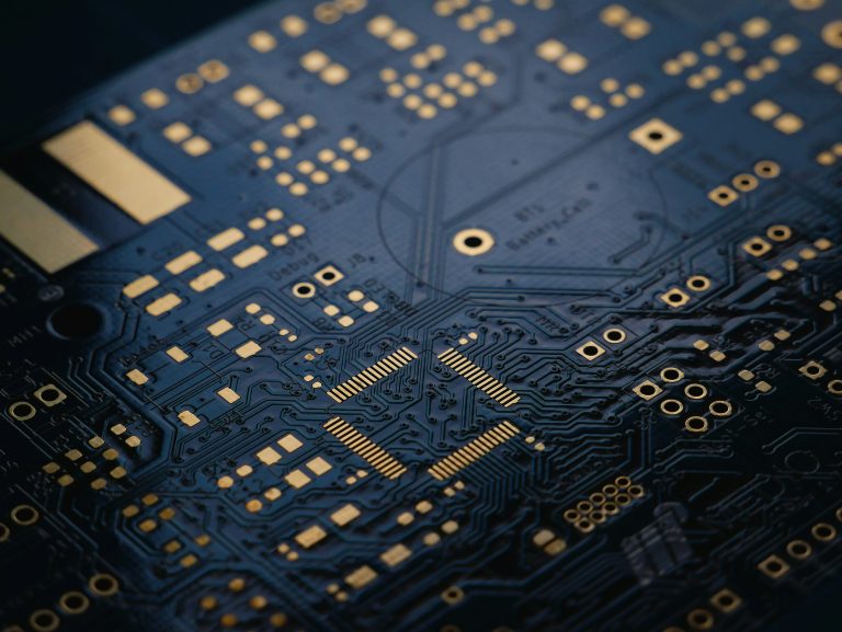
3. Inner Layer Imaging & Precision Etching
In high-speed PCB manufacturing, inner layers carry most high-speed signal traces, power planes, and ground planes, making imaging and etching one of the most decisive stages for signal stability.
Basic Working Principle
Copper-clad laminates are coated with photosensitive dry film, exposed under UV light, and chemically developed to retain designed circuit patterns. Excess copper is removed through controlled etching, followed by dry film stripping to form clean, accurate inner-layer circuitry.
Critical Control Parameters
| Parameter | Requirement | Impact on High-Speed PCB Manufacturing |
|---|---|---|
| Line width accuracy | ±10% (standard), ±7% (tight) | Directly affects characteristic impedance |
| Etching compensation | 0.5–1.5 mil | Counteracts side etching during processing |
| Layer-to-layer registration | ±2 mil (standard), ±1.5 mil (tight) | Prevents via misalignment and crosstalk |
Etching Compensation Explained
Side etching naturally occurs when etching solution erodes copper both vertically and horizontally, creating trapezoidal trace cross-sections. In high-speed PCB manufacturing, manufacturers calculate customized etching compensation based on copper foil thickness, solution concentration, and production speed.
AOI Automated Optical Inspection
After inner layer etching, high-resolution AOI scanners fully check for opens, shorts, trace notches, and residual copper. Full optical inspection captures hidden defects early, preventing faulty inner layers from entering lamination and lowering overall yield in high-speed PCB manufacturing.
4. Multilayer Lamination & Sequential Build-Up
Multilayer lamination merges separate inner layers, insulating prepreg, and outer copper foil into an integrated stackup. This stage of high-speed PCB manufacturing directly impacts impedance consistency.
Standard Lamination Workflow
Copper surface brownization → precise layer pre-stacking → high-temperature & high-pressure lamination → post-curing stabilization
Brownization forms a micro-rough oxide layer on copper surfaces, strengthening bonding between copper and resin. The temperature curve is customized according to material Tg values, with strictly controlled heating and cooling rates.
Why Lamination Impacts Performance
| Factor | Impact on High-Speed PCB Manufacturing |
|---|---|
| Uniform dielectric thickness | Directly stabilizes impedance for differential pairs |
| Accurate layer alignment | Eliminates via offset and reduces crosstalk |
| Controlled resin flow | Prevents uneven insulation thickness |
| Strong adhesion | Prevents layer separation in harsh environments |
The Cost Model: Why Lamination Cycles Matter
Each sequential lamination cycle adds significant cost to high-speed PCB manufacturing. Every cycle requires additional drilling, plating, and lamination. Reducing cycles by one can cut 15–25% from the fabrication cost of complex HDI boards.
Sequential Lamination for Complex Stackups
Unlike one-time lamination for traditional boards, sequential lamination uses multiple rounds of pressing, drilling, and plating to achieve high-density interconnection:
| Structure | Description | Typical Cycles | Application in High-Speed PCB Manufacturing |
|---|---|---|---|
| 1+N+1 | Single-sided blind vias top and bottom | 2 | Mainstream high-speed designs |
| 2+N+2 | Two-stage staggered blind vias | 3 | High-end server and computing hardware |
| Any-layer | Full arbitrary layer conduction | 4+ | Miniaturized, high-density devices |
This build-up method shortens signal paths, reduces parasitic capacitance, and is indispensable for 25Gbps+ transmission in high-speed PCB manufacturing.
5. Mechanical & Laser Drilling
In high-speed PCB manufacturing, vias enable interlayer conduction, and hole wall quality directly influences high-frequency performance due to the skin effect.
Mechanical Drilling
This method is ideal for apertures ≥0.2mm, offering stable cost efficiency. Standard hole position accuracy reaches ±1 mil, while premium high-speed PCB manufacturing achieves ±0.5 mil precision.
Laser Drilling
This is the core process for HDI microvias under 0.1mm:
| Laser Type | Best For | Key Advantage |
|---|---|---|
| CO₂ Laser | Insulating material microvia fabrication | Fast and efficient |
| UV Laser | Microvias in dense BGA areas | Ultra-fine focusing, low taper angle |
Laser drilling eliminates mechanical contact stress, avoiding substrate cracking in high-density high-speed PCB manufacturing.
Core Drilling Capabilities
| Parameter | Standard | Advanced High-Speed PCB Manufacturing |
|---|---|---|
| Minimum Mechanical Hole | 0.2mm (8 mil) | 0.15mm (6 mil) |
| Minimum Laser Microvia | 0.1mm (4 mil) | 0.075mm (3 mil) |
| Maximum Aspect Ratio | 10:1 | 15:1 |
| Hole Position Precision | ±1 mil | ±0.5 mil |
Desmear & Hole Wall Quality
Drilling leaves carbonized resin residue on hole walls. Professional desmear treatment removes contamination and enhances copper bonding. Smooth hole walls lower high-frequency resistance and signal loss in high-speed PCB manufacturing.
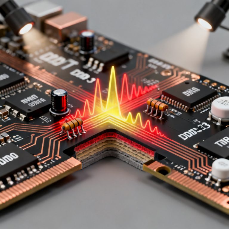
6. Back Drilling: Via Stub Elimination
Back drilling is a critical process in high-speed PCB manufacturing for multilayer boards operating above 10 Gbps. This technique eliminates signal interference caused by unused via stubs.
What Is It and Why Does It Matter?
After conventional through-hole drilling and plating, back drilling uses depth-controlled secondary drilling to remove redundant copper from non-functional layers. Shortening unused stubs eliminates high-frequency reflection, resonance noise, and eye diagram degradation.
The physics simply put: The stub behaves like an open-circuited transmission line. When its length reaches one-quarter of the signal’s wavelength, it creates an impedance null that blocks high-speed signals.
When Is This Technique Required?
| Signal Rate | Requirement | Role in High-Speed PCB Manufacturing |
|---|---|---|
| Below 3 Gbps | Optional | Stub interference is minimal |
| 3–10 Gbps | Highly recommended | Clear eye diagram improvement |
| 10–25 Gbps | Mandatory | Stub causes significant degradation |
| 25–56 Gbps | Required on all high-speed vias | Deep back drilling with tight control |
| 112G PAM4+ | Strict + ultra-precision | ±0.05mm depth tolerance required |
Common high-speed standards:
- 10–28 Gbps: PCIe Gen 4/5, 25G Ethernet, USB 3.2
- 56 Gbps: PCIe Gen 6, 50G Ethernet, 56G PAM4 SerDes
- 112 Gbps: PCIe Gen 7, 112G PAM4, 800G Ethernet
Depth Control & Key Parameters
The goal is to leave a residual stub of 5–10 mils (0.13–0.25 mm). This balances signal performance and mechanical integrity.
| Parameter | Standard | Advanced High-Speed PCB Manufacturing |
|---|---|---|
| Depth tolerance | ±0.1 mm (±4 mil) | ±0.05 mm (±2 mil) |
| Minimum residual stub | 10 mil (0.25 mm) | 5 mil (0.13 mm) |
| Back drill layers | 1–6 layers | 8+ layers |
Six Key Advantages
- Reduces crosstalk and high-frequency coupling
- Maintains precise impedance matching
- Improves bandwidth and eye diagram quality
- Lowers bit error rates and enhances reliability
- Meets PCIe and Ethernet industry standards
- Optimizes layer stack symmetry
Eight Challenges and Solutions
| Challenge | Practical Solution |
|---|---|
| Added cost | Apply only to critical high-speed nets |
| Drill bit wear | Regular replacement and life monitoring |
| High precision demand | X-ray pre-scan + real-time verification |
| HDI limitation | Replace with blind microvias |
| Thick core difficulty | Optimize stackup or use backdrill-and-fill |
| Layer count threshold | Evaluate alternative via structures |
| Quality control difficulty | Automated depth measurement |
| Surface dimple | Avoid component pads on opposite side |
Process Flow
- Standard fabrication: Inner layer processing, lamination, primary drilling
- Precision back drilling: X-ray positioning, depth-controlled drilling
- Deburring & cleaning: Edge smoothing for soldermask
Design Guidelines
- Keep 8–10 mil clearance around back-drilled vias
- Mark clear target layers in fabrication drawings
- Add dedicated test coupons on panel edges
- Complete back drill layer tables for factory reference
7. Back Drilling vs. Blind/Buried Via: Decision Framework
Engineers often confuse back drilling with HDI blind buried via. The right choice depends on data rate, density, and budget in high-speed PCB manufacturing.
Signal Integrity Comparison
| Characteristic | Standard Through-Hole | Back Drilling | Blind/Buried Via |
|---|---|---|---|
| Typical stub length | 60–250 mil | 4–10 mil | <1 mil |
| Resonant frequency | 2–10 GHz | 30–60 GHz | >100 GHz |
| Impedance discontinuity | High | Low | Very low |
| Parasitic capacitance | 0.5–1.0 pF | 0.1–0.2 pF | <0.05 pF |
Cost, Lead Time & Scalability
| Metric | Standard PTH | Back Drilling | Blind/Buried Via |
|---|---|---|---|
| Cost adder | Baseline | +10% to +20% | +30% to +100% |
| Lead time impact | Baseline | +1–2 days | +5–10 days |
| Yield risk | Low | Low to medium | Medium to high |
Rate-Based Selection Guide
| Data Rate | Recommended Strategy |
|---|---|
| <5 Gbps | Standard PTH |
| 5–10 Gbps | Back drilling |
| 10–28 Gbps | Back drilling (first choice) |
| 28–56 Gbps | Blind buried via |
| 56–112 Gbps+ | HDI microvias + fill |
Core takeaway: Back drilling is the most cost-effective upgrade for mainstream high-speed PCB manufacturing. HDI blind buried via is essential for ultra-high-speed products.
8. HDI Technology & Microvia Manufacturing
High Density Interconnect (HDI process) is essential for compact, high-density high-speed PCB manufacturing. This approach is required when line/space falls below 4/4 mil or BGA pitch drops below 0.5 mm.
Blind vs. Buried Via Differences
| Type | Fabrication Method |
|---|---|
| Blind Vias | Laser drilling + sequential lamination |
| Buried Vias | Inner core drilling before final lamination |
HDI Structure Options
| Type | Typical Cycles | Application |
|---|---|---|
| 1+N+1 | 2 | Cost-effective consumer and industrial |
| 2+N+2 | 3 | High-end server, BGA high-density |
| Any-layer | 4+ | Wearable, medical, miniaturized |
Microvia Reliability
| Risk | Mitigation |
|---|---|
| Corner cracking | Copper-filled vias for stacked structures |
| Voiding | X-ray inspection and strict process control |
| CAF failure | High-reliability material selection |
9. Plating and Hole Metallization
Plating quality ensures long-term reliability in high-speed PCB manufacturing.
Key targets:
- Average hole copper: ≥20μm
- Minimum: ≥18μm
- Uniformity: ±15%
Complete Plating Process
Desmear activation → electroless copper → full-board electroplating → pattern electroplating
High Aspect Ratio Solution
For vias with aspect ratio over 8:1, pulse electroplating optimizes ion circulation, ensuring balanced copper coverage for thick multilayer high-speed PCB manufacturing.
10. Solder Mask Application
Solder mask acts as the primary protective outer layer in high-speed PCB manufacturing.
Solder Mask Bridge Limitations
| BGA Pitch | Bridge Feasibility |
|---|---|
| ≥0.8 mm | Stable mass production |
| 0.65 mm | Precision alignment required |
| 0.5 mm | Custom high-precision processing |
| ≤0.4 mm | Not feasible; use NSMD pad design |
11. Surface Finish Selection Guide
| Finish | Best For |
|---|---|
| ENIG | BGA packaging, general high-speed |
| ENEPIG | 5G, millimeter-wave, high-precision |
| OSP | Cost-sensitive medium-speed |
| Hard Gold | Gold finger connectors |
Recommendation: For high-speed PCB manufacturing above 10 Gbps, ENIG and ENEPIG are the recommended options.
12. Impedance Control in Mass Production
Impedance control fabrication is the core benchmark of quality in high-speed PCB manufacturing.
Tolerance Grading
| Grade | Tolerance | Application |
|---|---|---|
| Standard | ±10% | Commercial communication |
| Tight | ±7% | Server backplanes, 10G–25G modules |
| Precision | ±5% | 56G/112G PAM4 ultra-high-speed |
13. Inspection, Testing & IPC Compliance
Final Electrical Testing
| Method | Application |
|---|---|
| TDR | Impedance verification |
| VNA | Insertion loss and crosstalk |
| Flying probe | Continuity and isolation |
| Four-wire Kelvin | Low-resistance detection |
All high-speed PCB manufacturing complies with IPC-A-600, IPC-6012, and IPC-2141.
14. High-Speed PCB Manufacturing Capability Table
| Parameter | Standard | Advanced |
|---|---|---|
| Layer Count | 2–32 Layers | 34+ Layers |
| Min Line / Space | 4/4 mil (0.1mm) | 3/3 mil, 2/2 mil |
| Min Mechanical Drill | 0.2mm (8 mil) | 0.15mm (6 mil) |
| Min Laser Microvia | 0.1mm (4 mil) | 0.075mm (3 mil) |
| Back Drill Tolerance | ±0.1mm | ±0.05mm |
| Impedance Tolerance | ±10% | ±7% / ±5% |
| HDI Support | 1+N+1, 2+N+2 | Any-Layer |
15. Industry Applications
High-speed PCB manufacturing serves:
| Industry | Data Rate | Key Demands |
|---|---|---|
| Data Communications | 10–112 Gbps | Back drilling + impedance control |
| Telecommunications | 10–56 Gbps | Low-loss material + ENEPIG |
| Aerospace & Defense | 1–40 GHz | IPC Class 3 high reliability |
| Automotive | 1–25 Gbps | Thermal cycling & CAF resistance |
16. Core Takeaways
- High-speed PCB manufacturing is a systematic project focusing on signal integrity
- Back drilling offers the best cost-performance for 10–28 Gbps designs
- Data rate determines via selection
- Impedance control depends on stackup design and process calibration
- IPC compliance indicates reliable suppliers
17. Frequently Asked Questions
Q1: What is high-speed PCB manufacturing?
A: It is precision PCB production for high-frequency signals, emphasizing impedance control, back drilling, and HDI technology.
Q2: Is back drilling required for 10Gbps signals?
A: Yes. This technique is mandatory for 10–28 Gbps signals in high-speed PCB manufacturing.
Q3: What is impedance control fabrication?
A: It is the core system that stabilizes target impedance using coupons and TDR testing.
Q4: What is HDI process?
A: High Density Interconnect uses blind/buried vias and sequential lamination.
Q5: What is blind buried via?
A: A microvia structure used in HDI to eliminate stubs for 28Gbps+ signals.
Q6: Do you provide TDR testing?
A: Yes. TDR impedance testing is standard in our high-speed PCB manufacturing service.
18. Custom High-Speed PCB Manufacturing & Quote
Whether you need prototype validation or mass production, our engineering team delivers one-stop customized solutions.
What We Provide
- Selective back drilling – ±0.1mm standard, ±0.05mm advanced
- Full HDI solutions – 1+N+1, 2+N+2, any-layer
- Graded impedance control – ±10%, ±7%, ±5%
- Complete testing – TDR, flying probe, four-wire Kelvin
Free Technical Support
We offer free DFM review, stackup optimization, and impedance verification.
Get Your Quote Within 24 Hours
Send us:
- Gerber files and stackup drawing
- Target impedance and tolerance
- Signal data rate and special process demands
- Order quantity and lead time
Contact our engineering team today to customize your high-speed PCB manufacturing solution.