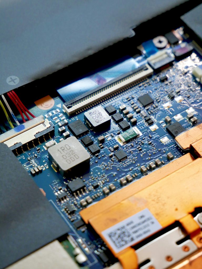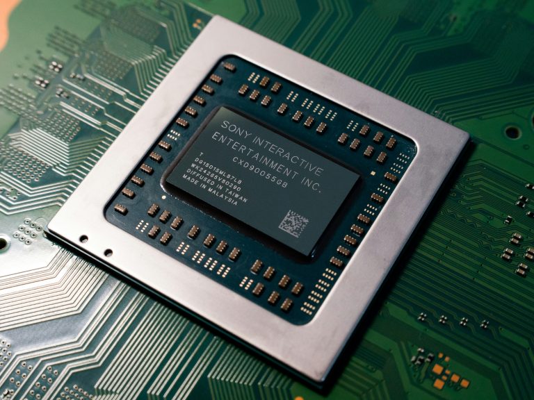
In modern electronics, high-speed PCB parameters define signal integrity, transmission stability, and mass-production reliability. From 1Gbps to 112G PAM4, 400G/800G links, and 77GHz radar, mastering high-speed PCB parameters helps you achieve consistent, high-performance circuit design.
Overview of High-Speed PCB Parameters
Understanding high-speed PCB parameters is essential for any high-bandwidth design. Unlike low-speed PCBs, high-speed systems require strict control over impedance, loss, materials, and tolerances. These high-speed PCB parameters form the foundation of stable signal transmission and long‑term reliability.
Why They Matter
Signal integrity depends entirely on consistent high-speed PCB parameters. Poor control causes reflection, attenuation, crosstalk, and bit errors, leading to unstable equipment operation.
Material selection relies on Dk/Df, Tg, and CTE values defined in high-speed PCB parameters to balance performance and cost.
Manufacturing cost is directly controlled by tolerance grades defined in high-speed PCB parameters, helping you choose cost‑effective solutions for consumer, industrial, automotive, and data center applications.
Four Core Categories
| Category | Core Indicators | Impact Scope |
|---|---|---|
| Electrical | Controlled impedance, insertion loss, return loss | Signal quality, channel budget |
| Material | Dk, Df, Tg, CTE | High-frequency performance, long-term reliability |
| Physical | Trace width/spacing, copper thickness, board thickness, aspect ratio | Manufacturability, current carrying capacity |
| Tolerance | Impedance tolerance, mechanical dimension tolerance, layer alignment | Mass production consistency, assembly accuracy |
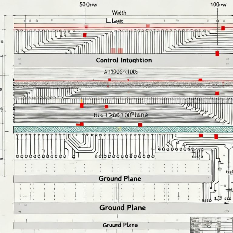
Controlled Impedance & Core Impedance Standards
Controlled impedance is one of the most important high-speed PCB parameters for reflection‑free signal transmission.
What is Characteristic Impedance (Z₀)?
Characteristic impedance is the instantaneous stable impedance encountered by high-speed signals during continuous propagation on transmission lines. It is a core part of high-speed PCB parameters and determined by trace geometry, dielectric thickness, and material Dk.
Core Formula:
Z0=CL
- L = Distributed inductance per unit length
- C = Distributed capacitance per unit length
- Unit: Ohm (Ω)
Key influence logic:
- Wider trace → Higher capacitance → Lower impedance
- Thicker dielectric → Lower capacitance → Higher impedance
- Higher Dk material → Stronger polarization → Lower impedance
Standard Impedance Values
Standard impedance values are universal across all high-speed PCB parameters and ensure compatibility between chips, connectors, and systems.
| Impedance Type | Standard Value | Typical Applications |
|---|---|---|
| Single-ended | 50Ω | High-speed signals, RF circuits, Wi-Fi, GPS |
| Single-ended | 75Ω | SDI video, broadcast signal transmission |
| Differential | 90Ω | USB 2.0, USB 3.x, USB4 differential pairs |
| Differential | 85Ω | Custom DDR5 high-speed memory channels |
| Differential | 100Ω | Ethernet, PCIe, HDMI, SATA, 100G/400G links |
| Differential | 120Ω | CAN bus, RS-485 industrial communication |
Impedance Tolerance Grading & Cost Impact
Impedance tolerance is a critical part of high-speed PCB parameters that directly affects yield and cost.
| Tolerance Grade | Deviation Range | Applicable Scenarios | Cost Impact |
|---|---|---|---|
| Standard | ±10% | Consumer electronics, general industrial control, below 10 Gbps | Baseline |
| Tight Controlled | ±7% | 25 Gbps+ communication, server motherboards, telecom backplanes | +10–15% |
| Precision | ±5% | 56G/112G PAM4, optical modules, 77GHz radar | +20–30% |
Key Factors Affecting Impedance
Four core design variables directly determine final performance:
| Variable | Change Trend | Effect on Impedance |
|---|---|---|
| Trace Width | Wider | Lower Z₀ |
| Dielectric Thickness | Thicker | Higher Z₀ |
| Dielectric Constant (Dk) | Higher | Lower Z₀ |
| Copper Thickness | Thicker | Slightly Lower Z₀ |
Differential Impedance Principle
Differential impedance is measured between two complementary signal pairs. Electromagnetic coupling exists between paired traces, so it cannot be calculated simply by single-ended impedance × 2.
Approximation Formula:
Zdiff≈2×Z0×(1−k)
- k = Electromagnetic coupling coefficient
- Loose coupling: Small k, differential impedance close to twice single-ended impedance
- Tight coupling: Large k, significantly reduced differential impedance
Common Impedance FAQ
| Question | Answer |
|---|---|
| Why is 50Ω the mainstream standard? | Balance of high-frequency loss, power load capacity, and manufacturing feasibility, universally recognized by RF and high-speed industries. |
| Can I customize non-standard impedance? | Yes, but it will increase cost, extend lead time, and reduce supplier compatibility. |
| What is the standard impedance test method? | TDR (Time Domain Reflectometry), compliant with IPC-TM-650. |
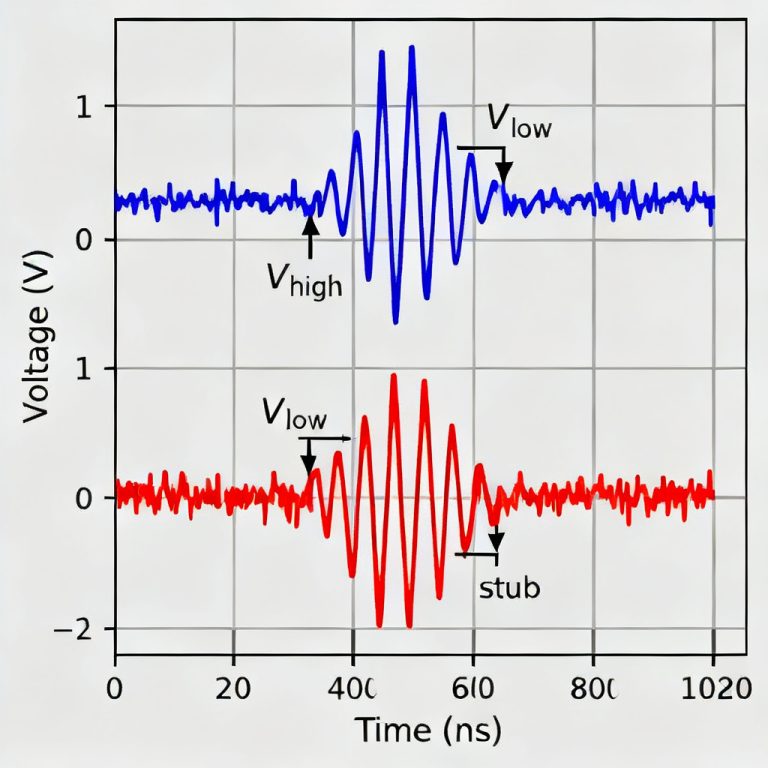
| Do vias affect high-speed impedance? | Yes. Uncontrolled via stubs cause impedance mutation; back-drilling is required for 10 Gbps+ signals. |
Insertion Loss & Return Loss
Loss parameters determine how far and how fast signals can travel. They are essential for high-bandwidth design.
Insertion Loss (IL) Definition & Calculation
Insertion loss refers to signal power attenuation during transmission through traces, vias, and connectors. Higher dB value means more serious signal attenuation.
Formula:
IL(dB)=−10×log10(PinPout)
With frequency increasing, skin effect and dielectric polarization intensify, and insertion loss rises rapidly.
Typical Insertion Loss Reference by Speed
| Signal Rate | Recommended Material Grade | Typical IL (dB/inch) | Channel Loss Budget |
|---|---|---|---|
| 1 Gbps | Standard FR4 | 0.10–0.20 | 10–15 dB |
| 3–5 Gbps | Mid-loss FR4 | 0.20–0.35 | 15–20 dB |
| 10 Gbps | Low-loss Laminate | 0.30–0.50 | 15–20 dB |
| 25 Gbps | Advanced Low-loss | 0.50–0.80 | 20–25 dB |
| 56 Gbps PAM4 | Ultra-low Loss | 0.80–1.20 | 25–30 dB |
| 112 Gbps PAM4 | Premium Ultra-low Loss | 1.20–1.80 | 30–35 dB |
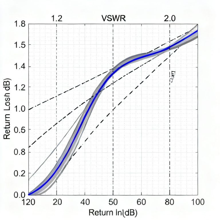
Return Loss (RL)
Return loss reflects signal reflection caused by impedance discontinuity, via defects, and unmatched terminals.
- Unit: dB (negative value)
- The more negative, the better performance
Industry standard requirements:
- Consumer electronics: -12 dB ~ -15 dB
- Telecom equipment: -15 dB ~ -20 dB
- 400G/800G high-end equipment: -20 dB ~ -25 dB
Three Major Components of High-Speed Loss
- Dielectric Loss: Determined by Df value, dominant above 5 Gbps.
- Conductor Loss: Caused by copper roughness and skin effect, obvious in low-frequency and ultra-high-frequency bands.
- Radiated Loss: EMI energy leakage, caused by incomplete reference plane and unreasonable wiring.
Insertion Loss vs. Return Loss Comparison
| Parameter | Excellent | Poor | Main Cause |
|---|---|---|---|
| Insertion Loss | <1 dB/in@10GHz | >2 dB/in@10GHz | High Df material, long trace, rough copper |
| Return Loss | <-20 dB | >-10 dB | Impedance mismatch, via discontinuity |
Key Material Indicators: Dk/Df, Tg & CTE
PCB substrate material performance determines the upper limit of high-speed signal capability. Dk, Df, Tg, and CTE must be clearly specified for all high-speed projects.
Dielectric Constant (Dk / εr)
Dk represents dielectric polarization capacity, affecting signal transmission speed and impedance stability.
| Material Type | Dk Range | High-Frequency Stability |
|---|---|---|
| Standard FR4 | 4.2–4.8 | Poor |
| Mid-loss FR4 | 4.0–4.4 | Moderate |
| Low-loss Laminate | 3.6–3.9 | Good |
| Ultra-low Loss Material | 3.4–3.7 | Very Good |
| PTFE High-frequency Material | 2.2–3.5 | Excellent |
Dissipation Factor (Df / tan δ)
Df is the core indicator of dielectric loss and the first selection standard for 25 Gbps+ high-speed PCB.
| Loss Grade | Df Range | Max Data Rate |
|---|---|---|
| Conventional | >0.020 | <1 Gbps |
| Mid-loss | 0.010–0.015 | 1–5 Gbps |
| Low-loss | 0.005–0.008 | 5–25 Gbps |
| Ultra-low loss | 0.001–0.005 | 25–112 Gbps |
Glass Transition Temperature (Tg)
Tg reflects high-temperature resistance of resin materials, directly affecting soldering resistance and board warpage.
| Tg Grade | Temperature | Application |
|---|---|---|
| Standard Tg | 130–140°C | Consumer low-speed products |
| Mid Tg | 150–160°C | General industrial equipment |
| High Tg | 170°C+ | Server, automotive, outdoor base station |
CTE (Coefficient of Thermal Expansion)
CTE refers to thermal expansion coefficient. Z-axis CTE is the key factor to avoid hole cracking and delamination during thermal cycling. Matching CTE between copper and dielectric ensures long-term reliability.
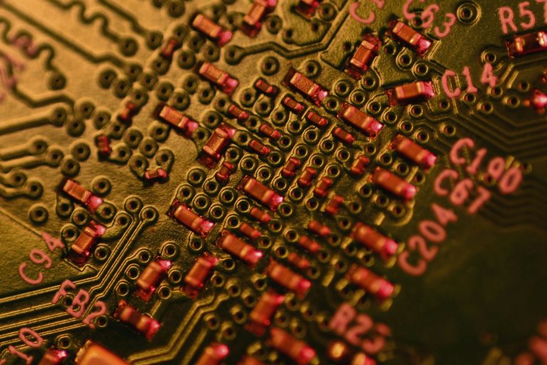
VLP & HVLP Copper Foil
Copper roughness directly affects high-frequency conductor loss.
| Copper Type | Roughness | Loss Performance | Application |
|---|---|---|---|
| Standard ED Copper | High | Baseline | Low-speed board |
| VLP Copper | Low | Optimized | 10–25 Gbps |
| HVLP Copper | Ultra-low | Best | 25–112 Gbps PAM4 |
Industrial Material Selection Guide
| Application | Dk | Max Df | Tg | Copper Recommendation |
|---|---|---|---|---|
| Consumer <5Gbps | 4.0–4.5 | <0.015 | 140°C+ | Standard ED |
| 10–25G Data Center | 3.4–3.8 | <0.008 | 170°C+ | VLP |
| 56G/112G Optical Module | 3.0–3.5 | <0.003 | 170°C+ | HVLP |
| 77GHz Automotive Radar | 2.2–3.5 | <0.002 | 170°C+ | HVLP / RA |
Critical Physical Specifications
Physical dimensions directly shape electrical performance.
Trace Width & Spacing
- Standard process: 4/4 mil
- High-density process: 3/3 mil
- Precision HDI: 2/2 milFine lines improve wiring density but require stricter impedance control.
Copper Thickness Specification
- 0.5 oz (17.5μm): Preferred for controlled signal layers
- 1.0 oz (35μm): Universal high-speed PCB
- 2.0 oz+: For high-power power layers
Board Thickness & Layer Count
- 4L: 0.8–1.6 mm
- 6–8L: 1.2–1.6 mm
- 10–12L: 1.6–2.0 mm
- Tolerance: ±10%
Aspect Ratio
- Standard capability: 10:1
- High-precision capability: 15:1Excessive aspect ratio will cause poor hole plating and reduce via reliability.
Industry Tolerance Standards & Grading
Tight tolerance ensures consistent performance in mass production.
Impedance Mass Production Tolerance
- ±10%: Standard process, widely available
- ±7%: Enhanced lamination + batch TDR test
- ±5%: Full inspection + customized stack-up
Universal Mechanical Tolerance
| Mechanical Item | Standard Tolerance |
|---|---|
| PCB outline dimension (routing) | ±0.2 mm |
| Drilled hole position (NC drill) | ±0.075 mm |
| Layer-to-layer registration | ±0.1 mm |
| Etched trace width (post-etch) | ±10% to ±15% |
Scenarios Requiring Tighter Tolerance
- Fine-pitch BGA (0.5 mm pitch and below)
- 25 Gbps+ ultra-high-speed serial signals
- Long channel wiring over 30 inches (760 mm)
- Strict insertion loss and return loss budget design
- Mass production projects with high AOI pass rate requirements
Testing Methods & Verification Indicators
Verification ensures your design meets performance goals.
TDR (Time Domain Reflectometry)
- Core function: Continuous impedance detection along traces; reveals exact location of discontinuities
- Output data: Impedance profile graph, maximum/minimum/average impedance values
- Accuracy: Up to ±5% of reading for calibrated instruments
- Industry standard: IPC-TM-650 2.5.5.11
VNA (Vector Network Analyzer)
- Core function: High-frequency test instrument for S-parameter measurement
- Test items: S11 (Return Loss), S21 (Insertion Loss), crosstalk, high-frequency isolation
- Frequency coverage: 10 MHz to 50 GHz+
- Output: IL vs. frequency plot; RL vs. frequency plot
Flying Probe Test
- What it measures: Electrical connectivity between nets (opens), isolation between neighboring nets (shorts)
- Coverage: Full-network open/short circuit detection – 100% circuit coverage
- Preferred for: Prototypes and low-volume production (no fixture cost)
What a Complete Test Report Includes
- Impedance (TDR): Target value, measured min/max/mean per trace, pass/fail for all high-speed lines
- TDR curve: Complete graph of impedance vs. distance
- Insertion loss (VNA): Fixed-frequency IL at Nyquist
- Return loss (VNA): Best, worst, and average RL across frequency band
- Microsection (optional): Cross-section photos showing hole wall copper thickness, layer alignment
Application-Based Selection Guide
Use this table as your starting point. Always verify with your specific component vendor and protocol specification.
| Application | Impedance Standard | Data Rate | Material Loss Grade | Max Df | Critical Control Points |
|---|---|---|---|---|---|
| USB 3.2 | 90Ω differential | 10 Gbps | Mid–Low loss | < 0.010 | Intra-pair length matching |
| USB4 | 90Ω differential | 40 Gbps | Low loss | < 0.008 | Strict equal length and low crosstalk |
| PCIe 4.0 | 100Ω differential | 16 GT/s | Mid–Low loss | < 0.010 | Insertion loss control at 8 GHz |
| PCIe 5.0 | 100Ω differential | 32 GT/s | Low loss | < 0.008 | IL + RL dual control at 16 GHz |
| PCIe 6.0 | 100Ω differential | 64 GT/s (PAM4) | Ultra-low loss | < 0.005 | Full parameter precision control |
| DDR4 | 40–60Ω single-ended | 3.2 Gbps | Standard FR4 | < 0.020 | Reference plane continuity and length matching |
| DDR5 | 40–60Ω single-ended | 6.4 Gbps | Mid–Low loss | < 0.012 | Tighter per-bit de-skew |
| 100G Ethernet (4 lanes) | 100Ω differential | 25 Gbps/lane | Low–Ultra-low loss | < 0.008 | Whole channel loss budget |
| 400G (PAM4) | 100Ω differential | 56 G/lane | Ultra-low loss | < 0.003 | Full-link impedance consistency |
| 800G (PAM4) | 100Ω differential | 112 G/lane | Ultra-low loss | < 0.002 | Extreme control of every parameter |
| 77 GHz Automotive Radar | 50Ω single-ended | Millimeter-wave | Ultra-low loss | < 0.002 | Df and Dk high-frequency stability over temperature |
How to Specify to Your PCB Vendor
Vague specifications lead to inconsistent results. Use this checklist to write a complete, unambiguous stack-up specification.
Mandatory Items in Every Impedance Specification
| Required Item | Example |
|---|---|
| Target impedance(s) | 50Ω single-ended; 100Ω differential |
| Tolerance | ±10% (or ±7%, ±5% if required) |
| Test method | IPC-TM-650 2.5.5.11 (TDR) |
| Coupon location | On-panel coupon (edge or panel center) |
| PCB layers under test | All signal layers with controlled impedance |
| Number of traces per test | Minimum 5 per layer per impedance value |
Mandatory Items for Material Selection
| Required Item | Example |
|---|---|
| Laminate manufacturer and grade | Rogers RO4350B or Isola Megtron 6 |
| Dk value and test frequency | Dk = 3.48 ±0.05 at 10 GHz per IPC-TM-650 |
| Df value and test frequency | Df = 0.0037 maximum at 10 GHz |
| Tg (glass transition) | Tg ≥ 170°C (by DSC) |
| Copper foil type | VLP (Very Low Profile) on all signal layers |
| Prepreg stack | Clearly defined layer stack diagram with thicknesses |
Reference IPC Standards (Include in Your PO)
| Standard | Title | Relevance |
|---|---|---|
| IPC-6012 | Rigid PCB Qualification and Performance | Defines acceptance criteria for finished boards |
| IPC-TM-650 | Test Methods Manual | Defines how Dk, Df, and impedance are measured |
| IPC-4101 | Specification for Base Materials | Defines laminate slash sheets |
| IPC-4562 | Metal Foil Specification | Defines copper foil types (VLP, HVLP, etc.) |
💡 Pro Tip: Include this exact sentence in your purchase order: “Stack-up and impedance per attached drawing. All test methods per IPC-TM-650. Acceptance criteria per IPC-6012 Class 2/3. TDR impedance report required for all impedance-controlled layers.”
Key Takeaways
- Controlled impedance uses 50Ω single-ended and 100Ω differential as universal standards.
- Impedance tolerance ±10% is standard; ±5% is required for 112G PAM4.
- Df < 0.008 is mandatory for 25 Gbps+ high-bandwidth systems.
- VLP/HVLP copper reduces conductor loss in high-speed designs.
- Clear specification and standardized testing ensure your high-speed PCB parameters perform reliably.
Custom Consultation & Quotation Support
Are you an electronics design engineer, hardware developer, or international procurement buyer looking for accurate high-speed PCB solutions?
Our high-speed engineering team provides free one-stop technical support for global customers:
✅ Free controlled impedance calculation & customized parameter suggestion
✅ Multi-layer stack-up design and optimization
✅ High-speed substrate material comparison & cost-effective selection
✅ Channel loss budget analysis and signal integrity risk evaluation
✅ IPC-compliant tolerance specification customization
Send your design files, interface type and signal rate, application scenario, and any material preferences. Our team responds within 1 business day with professional parameter evaluation, manufacturing feasibility analysis, and competitive formal quotation.
FAQ
Q1: What are the most critical indicators for high-speed designs?
A: The most critical are controlled impedance, insertion loss, return loss, Dk/Df, and impedance tolerance.
Q2: What is controlled impedance used for?
A: It is used for high-speed signals like PCIe, USB4, Ethernet, RF, and radar to avoid reflection and ensure signal integrity.
Q3: What tolerance do I need for 25Gbps+?
A: ±7% is recommended; ±5% for 56G/112G PAM4 systems.
Q4: Why are Dk and Df important?
A: Dk affects impedance; Df determines high-frequency dielectric loss and channel distance.
Q5: How are these specs tested?
A: TDR measures characteristic impedance; VNA measures insertion loss and return loss per IPC standards.