In high-speed PCB design, the reflection coefficient and VSWR are fundamental metrics to quantify reflection in transmission lines. These parameters directly impact signal integrity, especially when impedance mismatches occur at critical interfaces. Understanding how to measure and interpret these values ensures reliable high-speed interconnects for your custom PCB projects.
The Physics of Reflection: Why It Matters in Transmission Lines
A transmission line, such as a microstrip or stripline on a PCB, has a characteristic impedance (Z₀), typically 50Ω or 100Ω differential. When the load impedance (Z_L) at the end of the line—such as a receiver input, connector, or via—does not match Z₀, a portion of the incident voltage wave is reflected back toward the source. This reflected wave interferes with the incident wave, creating standing waves along the line. The fundamental cause of reflection is the discontinuity in impedance. The reflected wave’s magnitude and phase relative to the incident wave are described by the reflection coefficient (Γ).
Defining the Reflection Coefficient (Γ)
The reflection coefficient is a complex number (magnitude and phase) that quantifies how much of the incident wave is reflected at the load.
Mathematical Definition of Reflection Coefficient
Γ = (Z_L – Z₀) / (Z_L + Z₀)
Where Z_L is the load impedance and Z₀ is the characteristic impedance of the transmission line. A perfectly matched load yields Γ = 0.
Key Characteristics of the Reflection Coefficient
The magnitude |Γ| ranges from 0 (perfect match, no reflection) to 1 (complete reflection, e.g., open or short circuit). The phase ∠Γ indicates the phase shift of the reflected wave. For a purely resistive load, if Z_L > Z₀, Γ is positive; if Z_L < Z₀, Γ is negative. For reactive loads (capacitors, inductors), Γ is complex, meaning the reflected wave is shifted in phase relative to the incident wave.
Practical Interpretation in PCB Design
A low |Γ| (e.g., < 0.1) indicates a good impedance match, ensuring minimal signal reflection. High |Γ| (e.g., > 0.3) leads to significant signal degradation, especially in high-speed digital systems where rise times are fast. In your high-speed PCB prototyping, achieving a low reflection coefficient is critical for maintaining signal integrity.
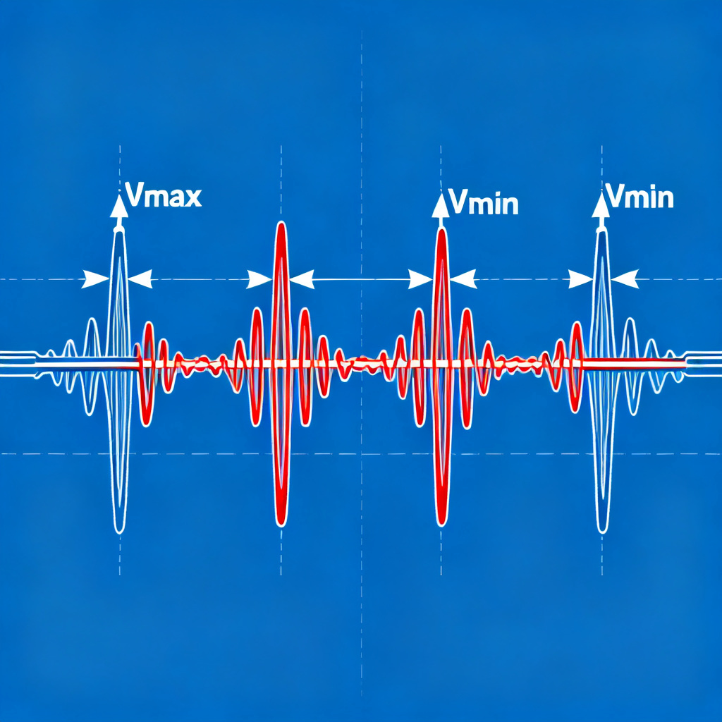
Voltage Standing Wave Ratio (VSWR)
While the reflection coefficient is fundamental, engineers often prefer VSWR for its intuitive interpretation of standing wave patterns.
Definition of VSWR
VSWR is the ratio of the maximum voltage amplitude to the minimum voltage amplitude along a transmission line, caused by the constructive and destructive interference of incident and reflected waves.
Mathematical Relationship Between VSWR and Reflection Coefficient
VSWR = V_max / V_min = (1 + |Γ|) / (1 – |Γ|)
Conversely, |Γ| = (VSWR – 1) / (VSWR + 1).
Key Characteristics of VSWR
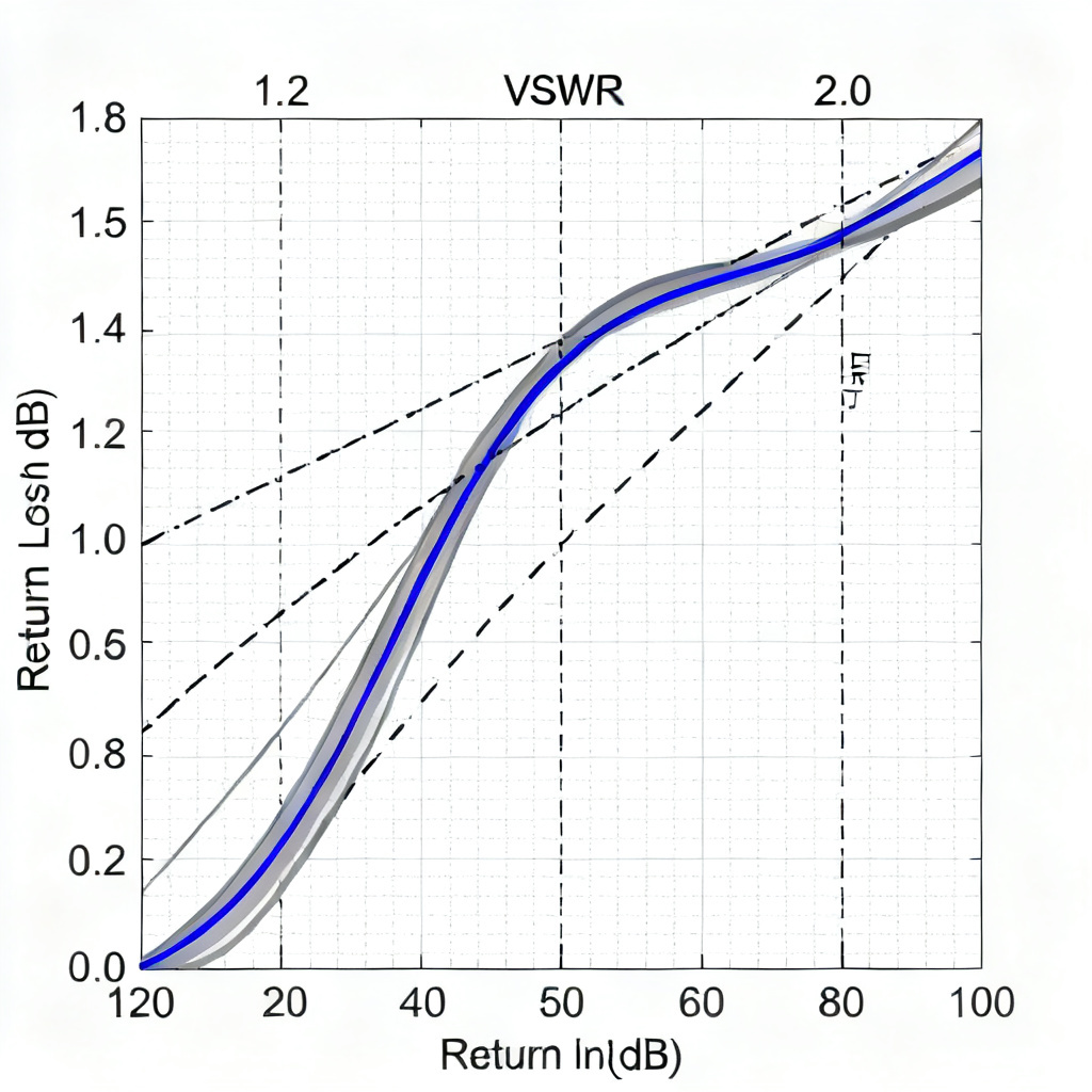
VSWR is always ≥ 1. A perfect match gives VSWR = 1 (no reflection). An open or short circuit yields VSWR = ∞ (complete reflection). In high-speed PCB design, VSWR < 1.2 is considered excellent (|Γ| < 0.09), while VSWR < 1.5 is typical for many interfaces (|Γ| < 0.2). VSWR > 2.0 indicates significant reflection issues (|Γ| > 0.33).
Why VSWR is Preferred in Some Contexts
VSWR provides a linear, positive scale that is easy to interpret when measuring antenna or transmission line performance. In RF and microwave engineering, VSWR is a standard specification for connectors, cables, and components.
Relationship Between Γ and VSWR: A Unified View
The reflection coefficient and VSWR are mathematically linked but offer different perspectives. The table below summarizes the relationship:
| Metric | Range | Interpretation |
|---|---|---|
| Reflection Coefficient (|Γ|) | 0 to 1 | Direct measure of reflected power. 0 = no reflection, 1 = total reflection. |
| VSWR | 1 to ∞ | Ratio of standing wave peaks to troughs. 1 = perfect match. |
Example Calculations for Reflection Coefficient and VSWR
- Perfect Match: Γ = 0, VSWR = 1
- 50Ω line with 75Ω load: Γ = (75-50)/(75+50) = 0.2, VSWR = (1+0.2)/(1-0.2) = 1.5
- Open Circuit: Γ = 1, VSWR = ∞
- Short Circuit: Γ = -1, VSWR = ∞
Return Loss (RL) as a Related Metric
Return Loss is expressed in dB: RL = -20 log₁₀(|Γ|). RL = 20 dB corresponds to |Γ| = 0.1 (10% reflected power), while RL = 10 dB corresponds to |Γ| = 0.316 (31.6% reflected power).
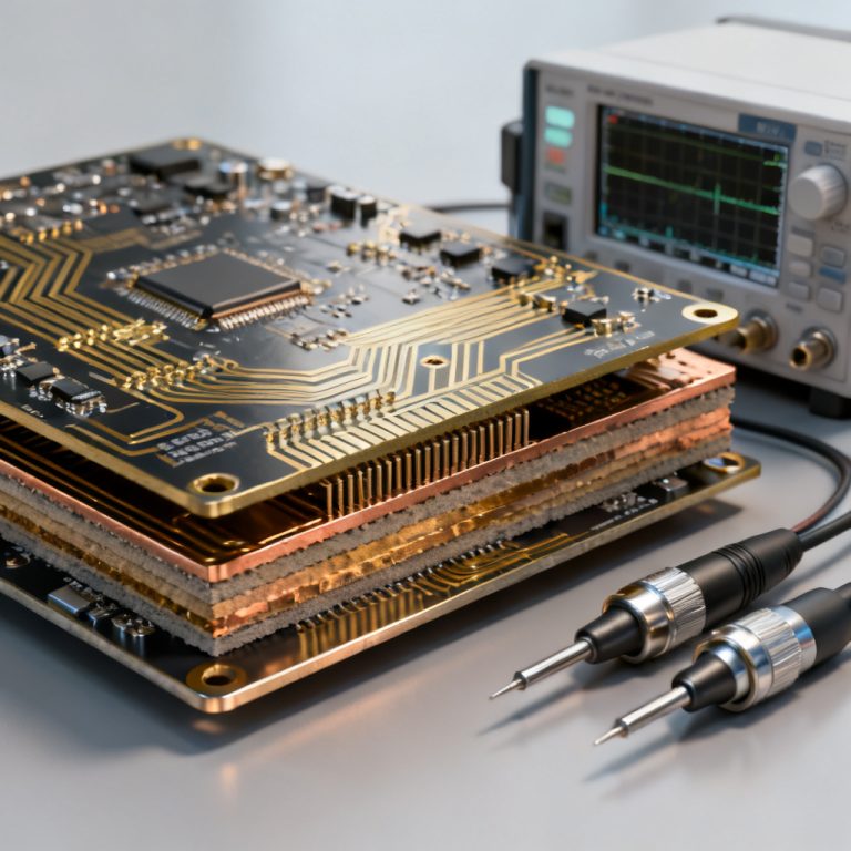
Practical Impact on High-Speed PCB Design
In your high-speed PCB designs, reflection directly affects signal integrity, eye diagram degradation, EMI, and power loss. Common sources of impedance mismatch in PCBs include stubs, vias, connectors, component pads, and trace width changes. For your custom high-speed PCB projects, minimizing these discontinuities is essential to keep the reflection coefficient and VSWR within acceptable limits.
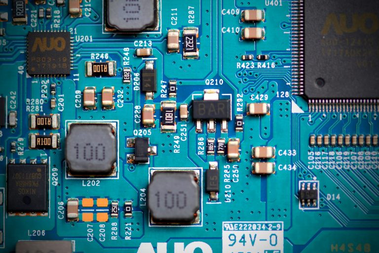
Common Sources of Impedance Mismatch in PCBs
- Stubs: Unused branches on a transmission line.
- Vias: Discontinuities in the reference plane or via barrel impedance.
- Connectors: Mismatch between PCB impedance and connector impedance.
- Component Pads: Capacitive loading from IC pins or package parasitics.
- Trace Width Changes: Neck-downs or width variations.
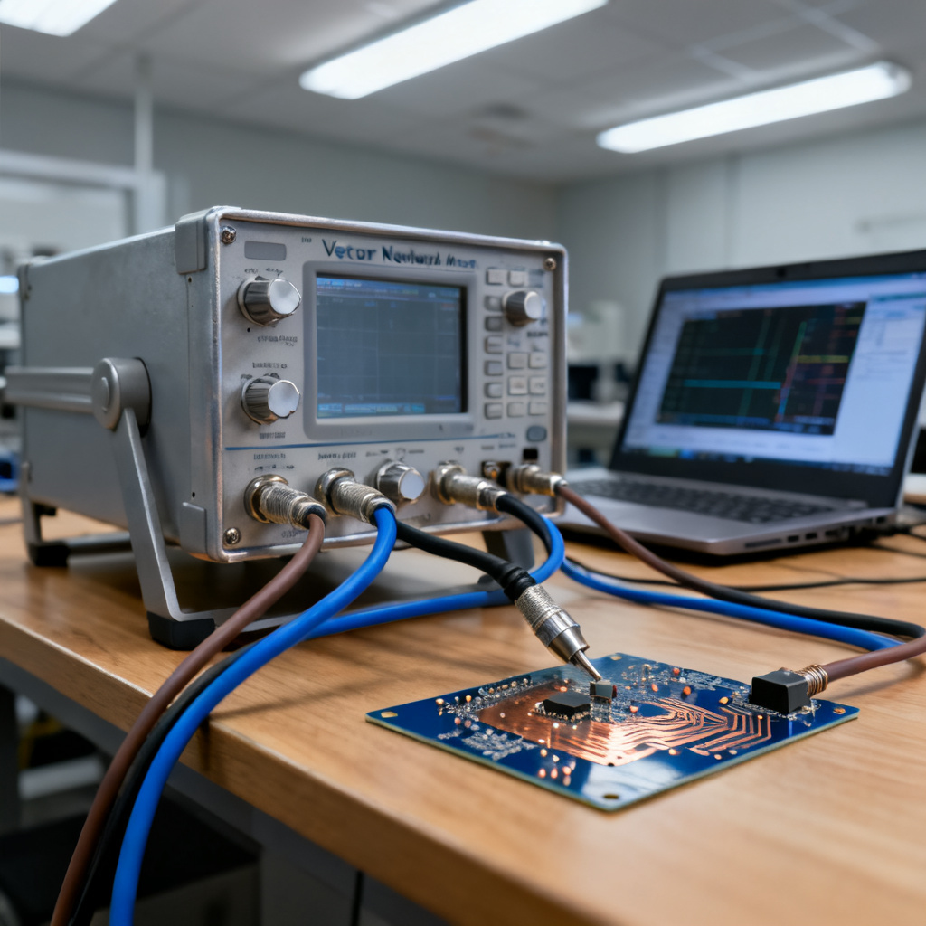
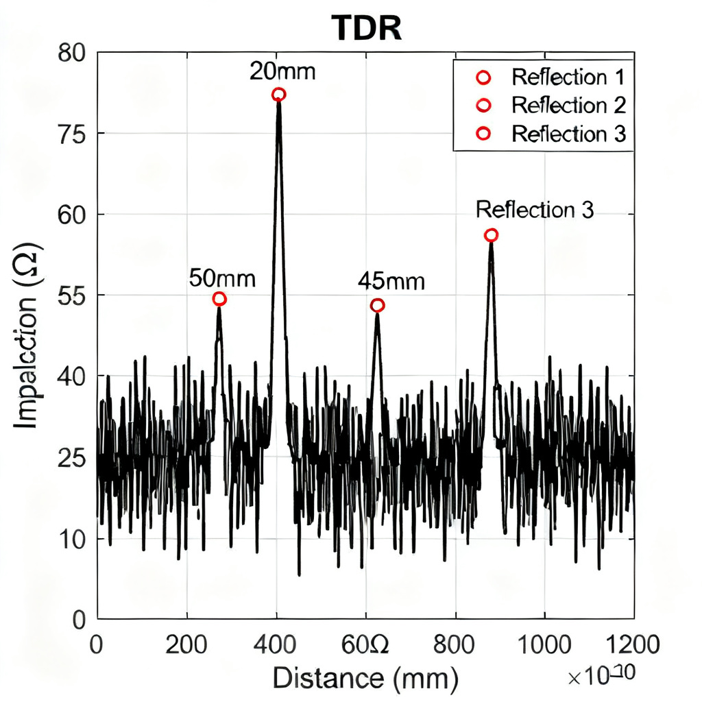
How to Measure and Simulate Γ and VSWR
Accurate measurement of the reflection coefficient and VSWR is crucial for validating your high-speed PCB designs.
Simulation Tools for Reflection Coefficient and VSWR
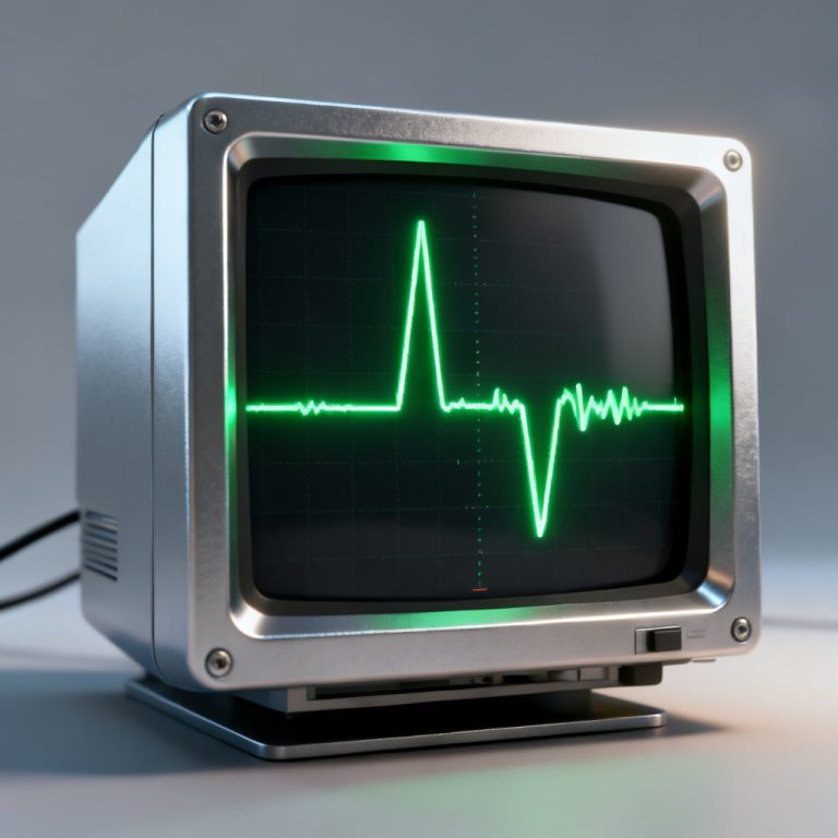
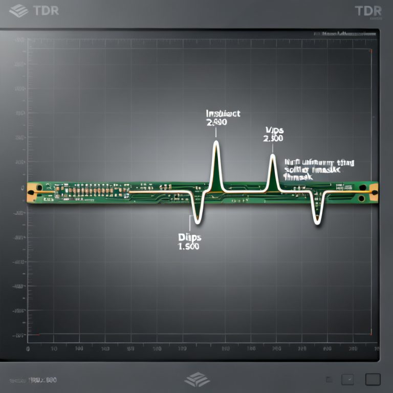
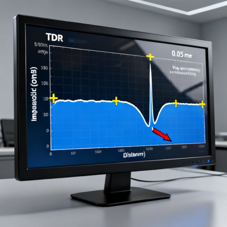
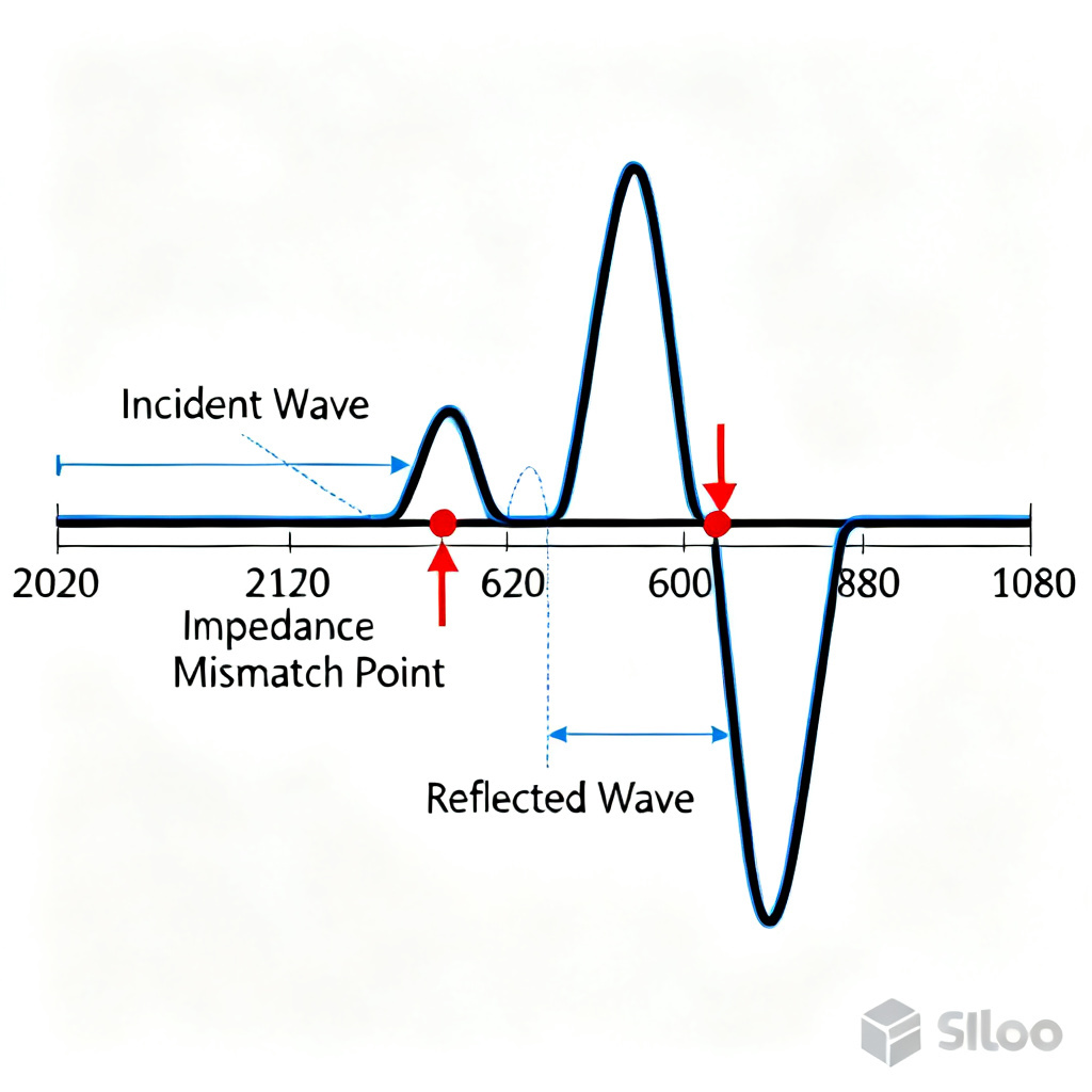
- Time Domain Reflectometry (TDR): Measures impedance profile along a line, directly showing reflection points.
- Frequency Domain (Vector Network Analyzer, VNA): Measures S-parameters, especially S11 (input reflection coefficient), from which VSWR is calculated.
- EM Simulators (e.g., Ansys HFSS, CST, Keysight ADS): Predict Γ and VSWR from PCB layout.
Measurement Techniques for Reflection Coefficient
Using a VNA, sweep frequency and measure S11. VSWR = (1+|S11|)/(1-|S11|). With TDR, apply a fast step pulse and observe reflected voltage: Γ = V_reflected / V_incident.
Interpreting Measurement Results
- Low VSWR (< 1.2): Excellent match; negligible reflections.
- Moderate VSWR (1.2–1.5): Acceptable for most high-speed digital signals up to 10 Gbps.
- High VSWR (> 2.0): Requires redesign (e.g., impedance tuning, stub removal, via optimization).
Design Guidelines to Minimize Reflections
To achieve low reflection coefficient and VSWR in your high-speed PCBs, follow these guidelines:
- Controlled Impedance: Specify impedance tolerance (e.g., 50Ω ± 10%) in your PCB stack-up. Work with your manufacturer to ensure consistent dielectric constant and trace geometry.
- Minimize Stubs: Use series termination or avoid long stubs. For critical nets, use daisy-chain routing.
- Optimize Vias: Use back-drilling to remove via stubs, or employ microvias for high-frequency signals.
- Match Connectors: Ensure connector impedance matches PCB impedance. Use differential pairs with correct spacing.
- Simulate Critical Nets: Run TDR or S-parameter simulations for high-speed interfaces (DDR, PCIe, SerDes).
- Use Termination Resistors: Place series or parallel termination at the source or load to absorb reflections.
Advanced Considerations for High-Speed Designers
For experienced designers working on high-speed PCB projects, additional factors influence the reflection coefficient and VSWR:
Frequency Dependence of Reflection Coefficient
Γ and VSWR vary with frequency. A design may have low VSWR at 1 GHz but high VSWR at 10 GHz due to skin effect, dielectric loss, or resonance. This is particularly important for high-speed serial links operating at 56G SerDes or 112G PCB design.
Differential Signaling Considerations
For differential pairs, use mixed-mode S-parameters. Differential VSWR is calculated from differential reflection coefficient (Sdd11). This is critical for PCIe 5.0 and other high-speed interfaces.
Time Domain vs. Frequency Domain Analysis
While VSWR is a frequency-domain metric, in digital systems, reflections are time-domain phenomena. Use TDR to see where reflections occur and VNA to quantify them at specific frequencies. For impedance control PCB validation, both methods are complementary.
Material Selection and Its Impact
Low-loss laminates (e.g., Rogers, Megtron) reduce attenuation, but impedance matching remains the dominant factor for reflection. The PCB Dk/Df values directly affect the characteristic impedance and thus the reflection coefficient.
Frequently Asked Questions
What is the difference between reflection coefficient and VSWR?
The reflection coefficient (Γ) directly measures the amount of reflected wave relative to the incident wave, while VSWR measures the ratio of maximum to minimum voltage along the transmission line. Both quantify impedance mismatch, but VSWR provides a more intuitive scale for standing wave patterns. In high-speed PCB design, understanding both metrics helps optimize signal integrity.
How do I calculate reflection coefficient from VSWR?
You can calculate the reflection coefficient magnitude from VSWR using the formula |Γ| = (VSWR – 1) / (VSWR + 1). For example, a VSWR of 1.5 corresponds to |Γ| = 0.2, indicating 20% of the incident wave is reflected. This is useful for impedance control PCB troubleshooting.
What is an acceptable VSWR for high-speed PCB designs?
For most high-speed digital designs, a VSWR below 1.2 is excellent, while VSWR below 1.5 is acceptable for signals up to 10 Gbps. For critical interfaces like PCIe 5.0 or 112G SerDes, targeting VSWR < 1.2 is recommended to ensure reliable data transmission. Your custom high-speed PCB should be designed with these targets in mind.
How does impedance mismatch affect signal integrity?
Impedance mismatch causes signal reflections, which lead to overshoot, undershoot, ringing, and non-monotonic edges. These effects degrade the eye diagram, reduce noise margins, and can cause data errors. By controlling the reflection coefficient and VSWR, you maintain signal integrity in your high-speed PCB designs.
What tools can I use to measure reflection coefficient?
Common tools include Time Domain Reflectometry (TDR) for time-domain analysis and Vector Network Analyzers (VNA) for frequency-domain S-parameter measurements. For simulation, tools like Polar Si9000, Ansys Q2D Extractor, and Saturn PCB Impedance Calculator help predict reflection coefficient before fabrication. These are essential for impedance control PCB simulation.