In high-speed PCB design, understanding transmission line reflection between source and load is critical for signal integrity. This pillar content explores whether source or load reflection matters more, providing actionable guidance for engineers designing high-speed digital and RF circuits.

Understanding Transmission Line Reflection Fundamentals
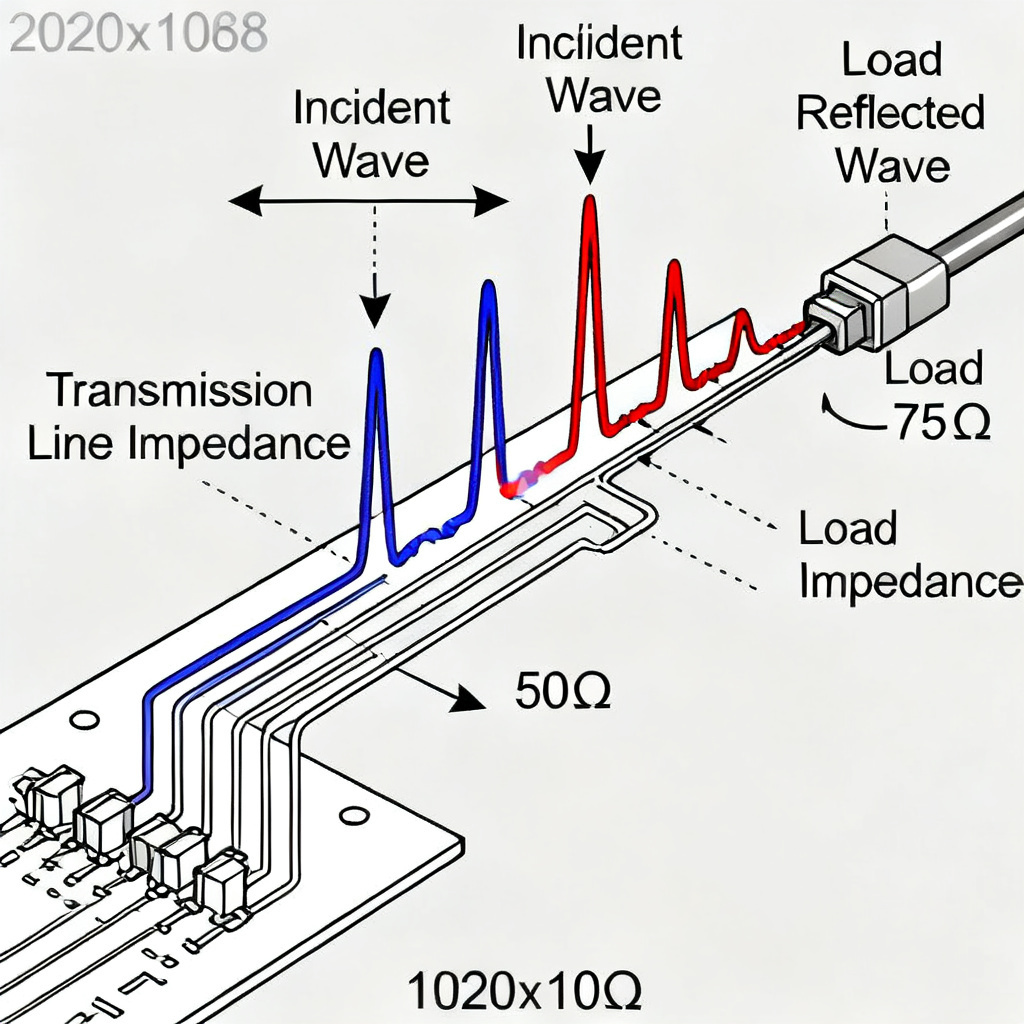
Transmission line reflection occurs when a signal encounters an impedance discontinuity, causing part of the energy to bounce back. The reflection coefficient (Γ) is defined as Γ = (Z_load – Z_0) / (Z_load + Z_0), where Z_0 is the characteristic impedance. For a high-speed PCB trace with Z_0 = 50Ω, a load of 100Ω gives Γ = +0.333 (33% reflected), while 25Ω gives Γ = -0.333. Reflections happen at both source and load ends, and their interaction determines overall signal quality.
Load Reflection in Transmission Lines
What is Load Reflection?
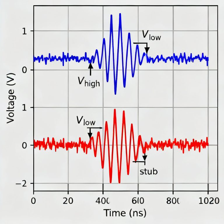
Load reflection occurs at the far end where the receiver sits. If the receiver’s input impedance doesn’t match Z_0, part of the incident signal reflects back toward the source. This directly affects the voltage waveform at the receiver, causing overshoot, undershoot, or ringing.
Why Load Reflection Matters
Load reflection determines signal integrity at the receiver. In a properly terminated system, the load absorbs all incident energy, eliminating reflection. For CMOS inputs with high impedance (Γ ≈ +1), the incident voltage doubles at the receiver—this is the classic “reflected wave switching” technique but also creates severe ringing. In differential pairs (LVDS, USB, HDMI), on-die termination minimizes load reflection. DDR memory uses ODT to match line impedance dynamically.
When Load Reflection Dominates
Load reflection is more critical when the receiver is far from the driver, the receiver’s input capacitance is significant, or the system uses “end termination” only. In point-to-point links with parallel termination at the load, load reflection is the primary concern.
Source Reflection in Transmission Lines
What is Source Reflection?
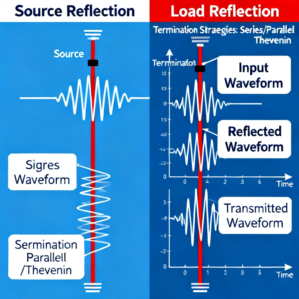
Source reflection happens at the driver end when the wave reflected from the load returns. If the driver’s output impedance doesn’t match Z_0, this returning wave is partially reflected back toward the load again, causing multiple reflections and sustained ringing.
Why Source Reflection Matters
Source reflection is the primary cause of sustained ringing. Each round trip adds another reflection, creating a staircase-like waveform. High source reflection can stress the driver with voltages outside supply rails, potentially damaging output stages. It also increases power consumption and EMI. Series termination at the source eliminates source reflection by making total source impedance equal to Z_0.
When Source Reflection Dominates
Source reflection is more critical when the driver is low-impedance, the line is long, or the system uses “source termination only.” In classic CMOS clock lines with series termination, source reflection absorbs the load’s reflected wave.
Source vs Load Reflection: Which Matters More?
The answer depends on topology. In point-to-point links with end termination (PCIe, SATA), load reflection matters more because the matched load prevents any reflected wave from reaching the source. In source-terminated systems, source reflection matters more because it absorbs the load’s reflection. In multi-drop buses, both matter equally, but load reflections from stubs dominate. For high-speed memory with ODT (DDR4, GDDR6), load reflection matters more during reads and writes.
Quantitative Comparison Table
| System Type | Critical Reflection | Reason |
|---|---|---|
| Single-ended, high impedance load | Load reflection | Voltage doubling at receiver |
| Differential, terminated at load | Load reflection | Matching is primary goal |
| Source-terminated, open load | Source reflection | Source absorbs reflected energy |
| Multi-drop bus | Load reflection (multiple) | Each stub creates its own reflection |
| DDR with ODT | Load reflection | ODT controls receiver reflection |
Termination Strategies for High-Speed PCB Reflection Control
Parallel Termination (Load Termination)
Parallel termination places a resistor at the receiver equal to Z_0, eliminating load reflection. Best for point-to-point links like PCIe and SATA. Drawback: DC power consumption.
Series Termination (Source Termination)
Series termination adds a resistor at the source to match Z_0, eliminating source reflection. Best for single-ended clocks and low-power designs. Drawback: Slower edge rate and voltage division.
Thevenin and AC Termination
Thevenin termination uses two resistors at the load for both DC bias and impedance matching. AC termination blocks DC power while matching high-frequency impedance. Both eliminate load reflection.
On-Die Termination (ODT)
ODT is integrated inside chips for DDR and high-speed memory interfaces, eliminating load reflection at the receiver. Programmable values (40Ω, 60Ω, 120Ω) allow dynamic matching.
Advanced Considerations for Transmission Line Reflection
Lossy Lines and Stub Effects
At GHz frequencies, dielectric losses attenuate reflected waves, making both source and load reflections less severe. Stubs in multi-drop topologies create distributed reflections that often dominate over both source and load reflections. Keep stub lengths < 1/10 of signal rise time.
Impedance Discontinuities from Vias and Connectors
Vias and connectors introduce parasitic capacitance and inductance, creating localized impedance mismatches. These generate reflections that are neither purely source nor load. Use back-drilling and controlled-impedance connectors.
Rise Time Impact
Faster rise times contain higher frequency components, making reflections more pronounced. Use the critical length rule: if line length > 1/6 of rise time electrical length, treat as transmission line.
Real-World Case Studies on Reflection
Case Study 1: 1 Gbps LVDS Link
Load reflection was the dominant issue with a 5% impedance mismatch at the receiver. Correcting load termination eliminated bit errors.
Case Study 2: 200 MHz Clock Distribution
Source termination alone couldn’t handle multiple loads. Adding parallel termination at the far end reduced overshoot from 40% to 5%.
Case Study 3: DDR4 Memory Bus
Stub reflections from the third DIMM dominated. Reducing stub lengths and adjusting ODT resolved read errors.
Design Guidelines for Transmission Line Reflection
- For point-to-point links: Load termination is critical; source termination optional.
- For source-terminated lines: Source termination mandatory; load reflection expected.
- For multi-drop buses: Minimize stub lengths; use Thevenin or AC termination.
- For high-speed memory: ODT at both ends; load reflection dominates.
FAQ: Transmission Line Reflection in High-Speed PCB
What is transmission line reflection in high-speed PCB?
Transmission line reflection is the partial return of signal energy due to impedance mismatches at source or load, causing signal degradation in high-speed PCB designs.
Does source or load reflection matter more for signal integrity?
For most high-speed PCB designs, load reflection matters more because it directly affects the receiver. However, source reflection is critical in source-terminated systems.
How do I minimize transmission line reflection?
Use proper termination: parallel at load for point-to-point links, series at source for clock lines, and ODT for memory interfaces. Match impedance within ±2%.
What tools measure transmission line reflection?
TDR (Time Domain Reflectometry) and VNA (Vector Network Analyzer) measure reflection coefficients. SPICE/IBIS simulations predict reflection behavior.
Can transmission line reflection damage drivers?
Yes, high source reflection can cause overshoot beyond supply rails, potentially damaging CMOS output stages in advanced nodes.
Conclusion: Load Reflection Dominates in High-Speed PCB
For most high-speed PCB designs, load reflection matters more than source reflection. The load is where the signal is received, and any distortion causes logic errors. Load termination is the most common solution, and modern standards assume load-side matching. However, source reflection cannot be ignored in source-terminated systems. The golden rule: always terminate the receiving side first, then add source termination if ringing persists.
Related High-Speed PCB Services
Our high-speed PCB fabrication services include controlled impedance manufacturing with ±2% tolerance, advanced stackup design, and signal integrity simulation. We specialize in custom high-speed PCB for applications up to 100 GHz, using materials like Rogers and Megtron. Contact us for your next high-speed PCB project.