Automating eye diagram PCB measurements using Python and VNA is the fastest method for high-speed PCB signal integrity validation. This guide provides a complete workflow for engineers who need accurate, repeatable results without manual oscilloscope testing.
Core Tools and Why This Matters for Eye Diagram PCB Measurements
Vector Network Analyzer vs. Oscilloscope
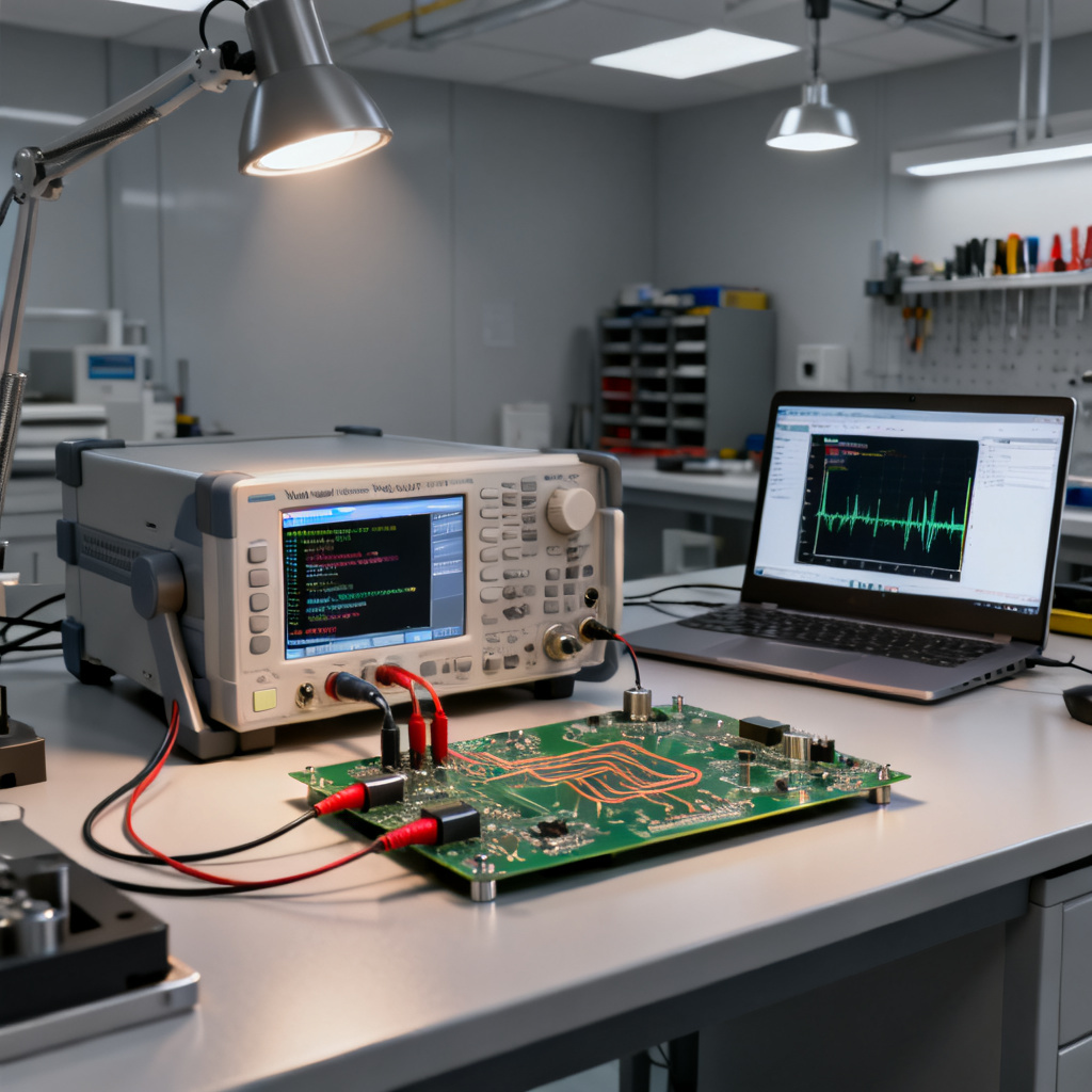
Traditional eye diagrams require a real-time oscilloscope and a high-speed signal generator. A VNA measures linear frequency-domain behavior (S-parameters) by sweeping a sine wave across a frequency range. This method characterizes the channel itself—the PCB trace, connector, and via—independent of specific data patterns. Once you have S-parameters, you can mathematically simulate any bit pattern to see how the channel distorts it.
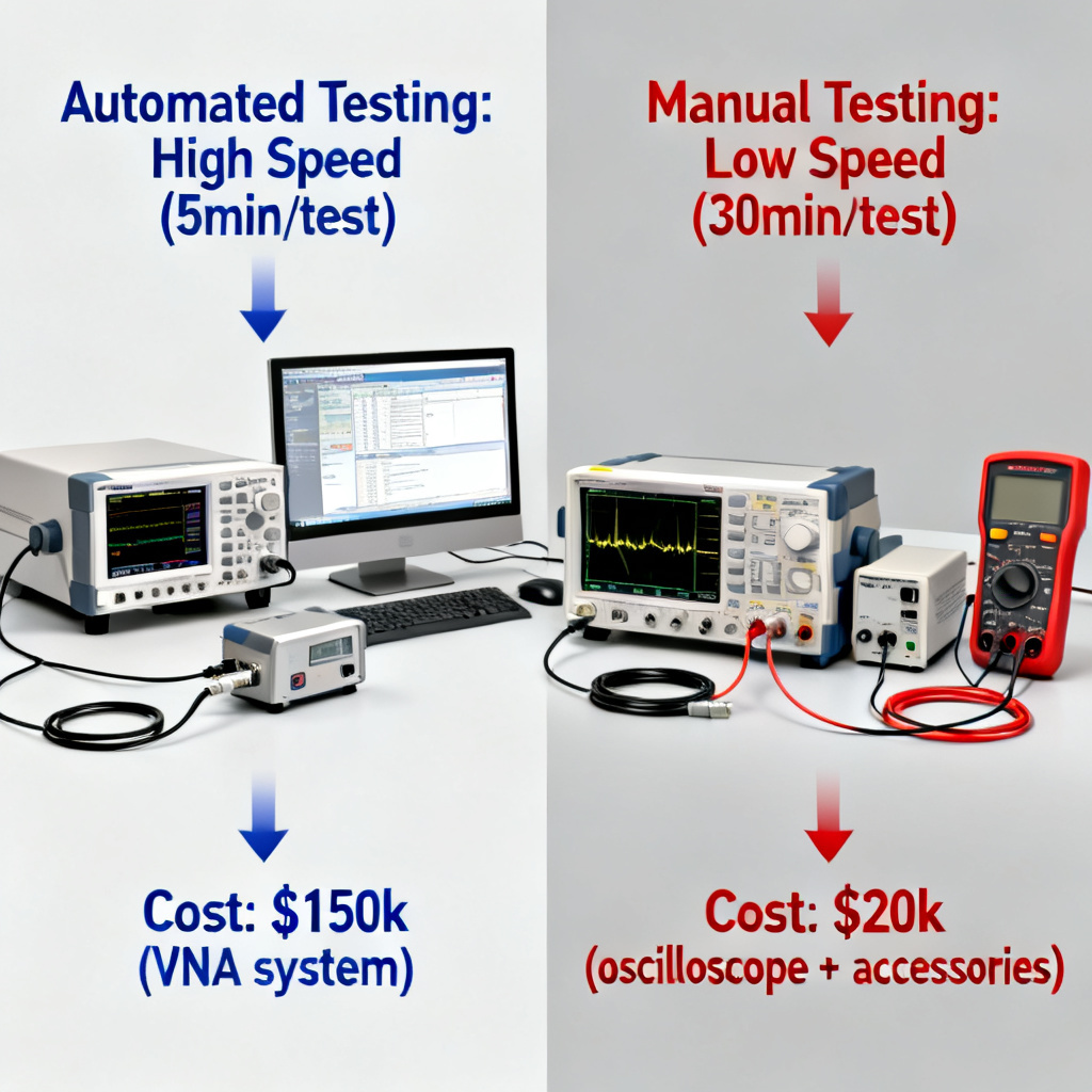
Automation with Python ensures every measurement uses the exact same frequency points, calibration, and analysis algorithm. This eliminates operator variability, a major source of error in manual oscilloscope measurements.
Python as Automation Controller
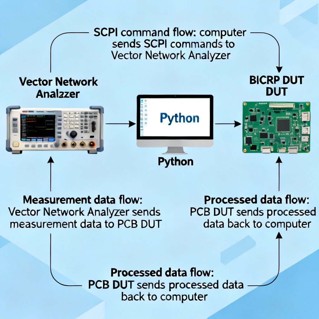
Python communicates with the VNA via SCPI commands over Ethernet, USB, or GPIB. Libraries like pyvisa, numpy, scipy, and matplotlib handle data acquisition, signal processing, and visualization. A Python script can connect to the VNA, set frequency range and power, trigger a measurement, download S21 data, process it to create an impulse response, convolve it with a PRBS, plot the eye diagram, and save results—all with one command.
Mathematical Foundation – From S-Parameters to Eye Diagram
Step 1: The Channel Impulse Response
The VNA measures S21 (forward transmission) in the frequency domain. To simulate a time-domain signal, apply an Inverse Fast Fourier Transform (IFFT) to the band-limited S21 data. Set the frequency span wide enough—at least 3-5 times the Nyquist frequency of your data rate. Set the number of frequency points high enough for fine time resolution. Apply a Kaiser window before the IFFT to reduce Gibbs phenomenon ringing.
import numpy as np
from scipy import signal
window = np.kaiser(len(S21_complex), beta=6)
S21_windowed = S21_complex * window
impulse_response = np.fft.ifft(S21_windowed)
impulse_response = np.fft.fftshift(impulse_response)
Step 2: Bit Pattern Generation
Generate a PRBS (Pseudo-Random Binary Sequence) such as PRBS7 or PRBS31. PRBS7 is suitable for PCIe Gen1/2, while PRBS31 is required for PCIe Gen4/5 and 100G Ethernet. Model the transmitter’s rise time by applying a low-pass filter to the ideal bit sequence.
def generate_prbs7():
    # Standard PRBS7 polynomial: x^7 + x^6 + 1
    return bit_sequence
bit_rate = 10e9
ui = 1 / bit_rate
samples_per_ui = 50
dt = ui / samples_per_ui
total_bits = 1000
time_vector = np.arange(0, total_bits * ui, dt)
ideal_signal = np.zeros_like(time_vector)
for i, bit in enumerate(bit_sequence[:total_bits]):
    start_idx = int(i * samples_per_ui)
    end_idx = int((i + 1) * samples_per_ui)
    ideal_signal[start_idx:end_idx] = bit
Step 3: Convolution and Eye Diagram Construction
Convolve the bit pattern with the channel’s impulse response to yield the simulated received waveform. Create the eye diagram by folding the waveform into 2-UI intervals and overlaying them. Simulate at least 100,000 to 1,000,000 bits for a statistically converged eye.
received_signal = np.convolve(ideal_signal, impulse_response, mode='same')
ui_samples = samples_per_ui
eye_traces = []
for i in range(ui_samples, len(received_signal) - 2*ui_samples, ui_samples):
    segment = received_signal[i : i + 2*ui_samples]
    eye_traces.append(segment)
import matplotlib.pyplot as plt
for trace in eye_traces[:500]:
    plt.plot(trace)
plt.xlabel('Time (samples)')
plt.ylabel('Voltage (V)')
plt.title('Automated Eye Diagram')
plt.show()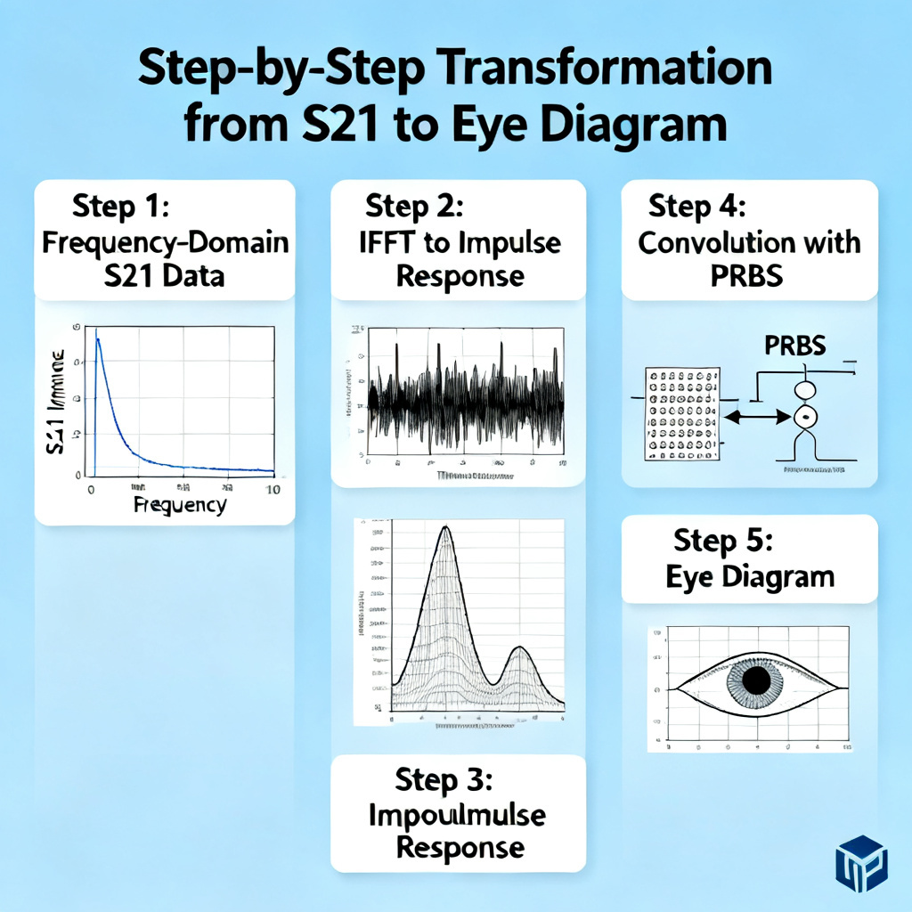
Complete Automation Workflow for Eye Diagram PCB Measurements
Hardware Setup
Use a 2-port or 4-port VNA with sufficient bandwidth (e.g., Keysight PNA, Rohde & Schwarz ZNB, Anritsu MS4647B). Perform a full 2-port SOLT calibration at the reference plane. Connect your high-speed PCB trace with appropriate connectors (SMA, 2.92mm, or GPPO).
Python Script Structure
Phase 1: VNA Initialization and Measurement
import pyvisa
rm = pyvisa.ResourceManager()
vna = rm.open_resource('TCPIP0::192.168.1.100::inst0::INSTR')
vna.write('*RST')
vna.timeout = 10000
vna.write(':SENS1:FREQ:START 10 MHz')
vna.write(':SENS1:FREQ:STOP 40 GHz')
vna.write(':SENS1:SWE:POIN 10001')
vna.write(':SENS1:BWID 1000 Hz')
vna.write(':INIT1:CONT OFF')
vna.write(':INIT1:IMM;*WAI')
vna.write(':CALC1:PAR:SDEF "MyS21", "S21"')
vna.write(':CALC1:PAR:SEL "MyS21"')
s21_data_str = vna.query(':CALC1:DATA:FDAT?')
s21_complex = np.fromstring(s21_data_str, sep=',').astype(complex)
Phase 2: Signal Processing
Apply windowing, IFFT, bit pattern generation, and convolution as described in the mathematical foundation section.
Phase 3: Eye Diagram Metrics Extraction
Automatically extract eye height, eye width, jitter (RMS and peak-to-peak), noise margin, and mask margin. Check if any trace violates the standard’s eye mask (e.g., PCIe, Ethernet).
Phase 4: Reporting and Logging
import datetime
timestamp = datetime.datetime.now().strftime("%Y%m%d_%H%M%S")
plt.savefig(f'eye_diagram_{timestamp}.png')
with open(f'measurements_{timestamp}.csv', 'w') as f:
    f.write('Metric,Value\n')
    f.write(f'Eye Height (V),{eye_height}\n')
    f.write(f'Eye Width (ps),{eye_width}\n')
    f.write(f'Jitter RMS (ps),{jitter_rms}\n')
np.savetxt(f's_params_{timestamp}.csv', np.column_stack((freq, np.real(s21_complex), np.imag(s21_complex))))
Advanced Considerations and Best Practices
Calibration is Everything
Poor VNA calibration is the single biggest source of error. Use a high-quality electronic calibration module or mechanical cal kit. Verify calibration with a known golden trace before measuring your DUT.
Dealing with Non-Linearities
This method assumes a Linear Time-Invariant (LTI) channel. This is valid for passive PCB traces but breaks down if active components like buffers, redrivers, or equalizers are included.
De-embedding
To get true trace performance, perform de-embedding using Python libraries like scikit-rf. Measure a separate calibration structure (open, short, thru) on the same PCB and remove fixture effects.
Correlation with Oscilloscope
Validate your automated method by comparing results with a real-time oscilloscope. Good correlation within 5-10% confirms your setup.
Key Metrics Table for Eye Diagram PCB Measurements
| Metric | Description | Typical Value (10 Gbps) |
|---|---|---|
| Eye Height | Vertical opening at center of eye | 200-400 mV |
| Eye Width | Horizontal opening at center of eye | 80-95 ps |
| Jitter RMS | Horizontal spread at crossing point | 1-5 ps |
| Noise Margin | Vertical spread at top/bottom of eye | 50-100 mV |
| Mask Margin | Distance from mask violation | >10% |
Comparison: VNA + Python vs. Oscilloscope for Eye Diagram PCB Measurements
| Aspect | VNA + Python Automation | Oscilloscope |
|---|---|---|
| Hardware Cost | Lower (one VNA for many tests) | Higher (requires signal generator) |
| Repeatability | High (automated script) | Moderate (operator dependent) |
| Speed | Fast (batch processing) | Slow (manual per measurement) |
| Channel Characterization | Full S-parameter data | Limited to specific patterns |
| Best For | Design validation, production testing | Final compliance testing |
Industry Terminology Explained
S-parameters: Scattering parameters that describe electrical behavior of linear networks in the frequency domain. S21 is forward transmission gain. IFFT: Inverse Fast Fourier Transform converts frequency-domain data to time-domain. PRBS: Pseudo-Random Binary Sequence used to simulate real-world data patterns. De-embedding: Removing fixture and cable effects from measurement data to isolate DUT performance. Eye mask: A standardized polygon on the eye diagram that the signal must not enter to ensure compliance.
FAQ
What is the advantage of automating eye diagram PCB measurements with Python and VNA?
Automating eye diagram PCB measurements with Python and VNA provides faster, more repeatable results compared to manual oscilloscope methods. It eliminates operator variability and enables batch testing of multiple traces.
Can this method replace an oscilloscope for final compliance testing?
While VNA + Python automation is excellent for design validation and production screening, final compliance testing often requires an oscilloscope per industry standards. However, the correlation between methods is very high when properly calibrated.
What VNA bandwidth do I need for 28 Gbps eye diagram PCB measurements?
For 28 Gbps signals, a VNA with at least 40 GHz bandwidth is recommended to capture the 5th harmonic and ensure accurate impulse response reconstruction.
How many bits should I simulate for a converged eye diagram?
Simulate at least 100,000 to 1,000,000 bits for a statistically converged eye diagram. This ensures realistic jitter and noise representation.
What is de-embedding and why is it important?
De-embedding removes the effects of cables, connectors, and launch structures from your measurement. It isolates the true performance of the PCB trace itself, which is critical for accurate eye diagram PCB measurements.