When designing high-speed PCBs, understanding crosstalk in High Speed PCB field solver setup is critical to maintaining signal integrity. This guide compares 2D, 2.5D, and 3D solvers for accurate crosstalk analysis.
1. Understanding Crosstalk Fundamentals in High Speed PCB
1.1 Capacitive and Inductive Coupling in High Speed PCB
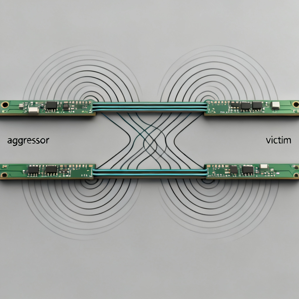
In any high-speed PCB, crosstalk arises from two physical mechanisms. Capacitive coupling occurs when a voltage change on the aggressor trace induces a displacement current into the victim trace through parasitic capacitance. This is dominant in high-impedance circuits. Inductive coupling happens when a changing current in the aggressor trace creates a magnetic field that induces a voltage via mutual inductance. This is dominant in low-impedance circuits.
1.2 Near-End vs. Far-End Crosstalk in High Speed PCB
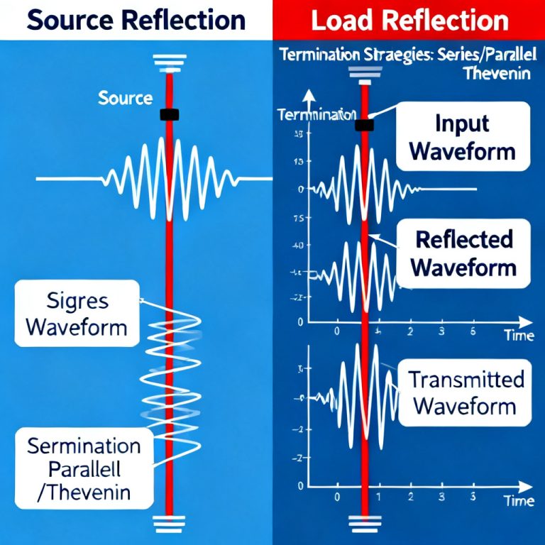
NEXT (Near-End Crosstalk) is measured at the end of the victim line closest to the aggressor driver. It is typically larger in magnitude and has a pulse width equal to twice the line’s propagation delay. FEXT (Far-End Crosstalk) is measured at the opposite end of the victim line. It is sensitive to the dielectric properties and trace geometry. FEXT can be reduced by using homogeneous dielectric materials and symmetric stripline structures.
1.3 Key Parameters a Field Solver Must Extract for High Speed PCB
To model crosstalk in high-speed PCB accurately, a solver must compute self-inductance (L11, L22), self-capacitance (C11, C22), mutual inductance (L12), mutual capacitance (C12), characteristic impedance (Z0), propagation delay (Tpd), and coupling coefficient (K = L12 / sqrt(L11*L22)).
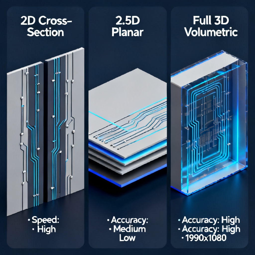
2. The 2D Field Solver for High Speed PCB Crosstalk
2.1 What is a 2D Solver for High Speed PCB?
A 2D field solver assumes PCB traces are infinitely long and uniform in the direction of signal propagation (Z-axis). It solves for cross-sectional electric and magnetic fields in the X-Y plane. This is the most common solver type for pre-layout analysis of crosstalk in high-speed PCB.
2.2 Strengths of 2D Solvers for High Speed PCB
Speed is the primary advantage—2D simulations complete in seconds, enabling rapid parametric sweeps of trace width, spacing, or dielectric thickness. Simplicity means no need to define 3D geometry or ports; only a cross-section stackup is required. For long, straight, uniform traces like backplane or memory bus traces, 2D solvers provide highly accurate RLCG matrices. They are ideal for stackup optimization before layout.
2.3 Limitations of 2D Solvers for High Speed PCB
2D solvers cannot model discontinuities like vias, bends, connectors, or tapered traces. Some handle frequency-dependent skin effect and dielectric loss, but many simpler tools do not. Edge effects are ignored, so coupling for traces near the board edge may be overestimated.
2.4 When to Use a 2D Solver for High Speed PCB Crosstalk
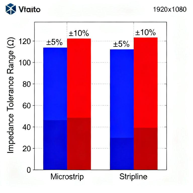
Use 2D solvers for pre-layout feasibility studies, determining minimum trace spacing for a given crosstalk budget (e.g., less than 1% NEXT), creating design rules for differential pairs, and initial calculations for microstrip vs. stripline crosstalk differences.
2.5 Example Setup for High Speed PCB (from Altium Documentation)
In a 2D solver like Altium’s SiWave or Polar, define the stackup with layer thickness, dielectric constant (Dk), and loss tangent (Df). Draw trace cross-sections with width, thickness, and copper roughness. Set solver options to quasi-static or full-wave for high frequencies. Run the simulation to get the RLCG matrix and crosstalk coefficients.
3. The 2.5D Field Solver for High Speed PCB Crosstalk
3.1 What is a 2.5D Solver for High Speed PCB?
A 2.5D solver is a full 3D electromagnetic solver that assumes the geometry is planar—all conductors lie on a flat substrate. It uses a method of moments (MoM) or similar technique to solve for currents on conductor surfaces. It is called 2.5D because the mesh is 2D on the plane, but fields are computed in 3D.
3.2 Strengths of 2.5D Solvers for High Speed PCB
2.5D solvers handle planar discontinuities like vias, pads, and small bends. They are more accurate than 2D by accounting for fringing fields and coupling between non-parallel traces. They are faster than full 3D for planar structures—tools like Keysight ADS Momentum, Sonnet, and Ansys HFSS 3D Layout are significantly faster than full 3D FEM solvers. Multiple ports can be defined to compute S-parameters including crosstalk (S31, S41).
3.3 Limitations of 2.5D Solvers for High Speed PCB
2.5D solvers cannot model true 3D structures like stacked vias through multiple layers, buried components, or non-planar geometries such as wire bonds or connectors. They assume an infinite ground plane, which may not reflect real board behavior. Fine details require very fine meshing, increasing simulation time.
3.4 When to Use a 2.5D Solver for High Speed PCB Crosstalk
Use 2.5D solvers for analyzing crosstalk between traces that cross a split plane, modeling via-to-via coupling in multi-layer PCBs, post-layout verification of critical nets, and differential pair crosstalk analysis with mild bends.
3.5 Example Setup for High Speed PCB (from Cadence Sigrity Documentation)
In a 2.5D solver like Cadence Sigrity 2.5D, import the PCB layout (ODB++ or IPC-2581). Define the stackup and material properties. Select nets of interest (aggressor and victim). Set the simulation frequency range (e.g., DC to 20 GHz). Choose the solver type: MoM or PEEC (Partial Element Equivalent Circuit). Extract S-parameters and view crosstalk vs. frequency plots.
4. The 3D Field Solver for High Speed PCB Crosstalk
4.1 What is a 3D Solver for High Speed PCB?
A 3D field solver solves Maxwell’s equations in all three spatial dimensions using Finite Element Method (FEM), Finite Difference Time Domain (FDTD), or Integral Equation (IE) methods. It discretizes the entire volume of the structure, including air, dielectric, and conductors.
4.2 Strengths of 3D Solvers for High Speed PCB
3D solvers handle any geometry: vias with backdrilling, BGA breakout patterns, connectors, cables, and non-ideal return paths. They provide full-wave accuracy, capturing resonances, radiation, and high-frequency effects like skin effect and dielectric dispersion. They can model crosstalk between traces on different layers, through vias, and across board edges. They support frequency-dependent Dk and Df, as well as anisotropic materials.
4.3 Limitations of 3D Solvers for High Speed PCB
Simulation time can be hours or days for complex structures. They require high-end workstations with large RAM (often over 64 GB) and multi-core processors. Port setup complexity—defining correct wave ports, lumped ports, and de-embedding—is non-trivial. Mesh convergence requires careful refinement; poor meshing leads to inaccurate crosstalk predictions.
4.4 When to Use a 3D Solver for High Speed PCB Crosstalk
Use 3D solvers for final sign-off on critical high-speed channels like PCIe Gen 5/6, DDR5, or 100G Ethernet. They are essential for modeling crosstalk through connectors or cable assemblies, analyzing via stub effects on crosstalk, investigating EMI from crosstalk, and validating 2D or 2.5D simulation results.
4.5 Example Setup for High Speed PCB (from Ansys HFSS Documentation)
In a 3D solver like Ansys HFSS, import 3D geometry from ECAD or MCAD tools. Assign materials: conductors (copper with roughness) and dielectrics (with Dk and Df). Define excitation ports: wave ports for transmission lines, lumped ports for IC pins. Set the solution frequency and adaptive mesh refinement. Solve for S-parameters and export crosstalk metrics (NEXT, FEXT, PSXT). Perform time-domain analysis via inverse FFT to see crosstalk waveforms.
5. Comparative Analysis: 2D vs 2.5D vs 3D for High Speed PCB
| Feature | 2D Solver | 2.5D Solver | 3D Solver |
|---|---|---|---|
| Geometry Assumption | Infinite uniform cross-section | Planar (2D mesh, 3D fields) | Full 3D volume |
| Simulation Speed | Seconds to minutes | Minutes to hours | Hours to days |
| Accuracy for High Speed PCB | Good for uniform traces | Good for planar discontinuities | Excellent for all geometries |
| Crosstalk Modeling | RLCG matrix only | S-parameters (NEXT/FEXT) | Full S-parameters + time domain |
| Best Use Case | Pre-layout rule creation | Post-layout verification | Final sign-off / complex structures |
| Tool Examples | Polar Si8000, Simbeor 2D | Keysight Momentum, Sonnet | Ansys HFSS, CST Studio, COMSOL |
Key insight from industry experts: Altium recommends starting with 2D for design rule generation, then moving to 2.5D for layout validation, and only using 3D for the most critical nets. Cadence emphasizes that 2.5D solvers are often sufficient for 90% of high-speed PCB crosstalk problems, provided the structure is planar. Sierra Circuits notes that for crosstalk between traces on the same layer, 2D is highly accurate; for via-to-via crosstalk, 2.5D or 3D is mandatory.
6. Practical Guidelines for Choosing the Right Solver for High Speed PCB
6.1 When to Choose 2D for High Speed PCB
Choose 2D when you are in the early design phase (pre-layout), need to determine minimum trace spacing for a given crosstalk budget, traces are long and uniform, or you are performing parametric sweeps.
6.2 When to Choose 2.5D for High Speed PCB
Choose 2.5D when you have a complete layout and need to verify crosstalk on critical nets, the design includes planar discontinuities, you need S-parameter extraction for channel simulation, or the board is a standard multi-layer PCB.
6.3 When to Choose 3D for High Speed PCB
Choose 3D when designing for ultra-high speeds above 56 Gbps PAM4, the structure includes connectors or BGA packages, you need to model crosstalk through multiple vias and layers, or you are performing EMI/EMC analysis.
6.4 Common Mistakes to Avoid in High Speed PCB
Avoid using 2D for via crosstalk, using 3D for everything, ignoring frequency dependence, and not de-embedding ports.
7. Advanced Topics in High Speed PCB Crosstalk
7.1 Crosstalk in Differential Pairs for High Speed PCB
Differential pairs inherently have lower crosstalk than single-ended traces due to field cancellation. However, intra-pair skew and impedance mismatch can degrade this advantage. Use 2.5D or 3D solvers to model differential-to-common mode conversion (Scd21) and mode conversion due to asymmetry.
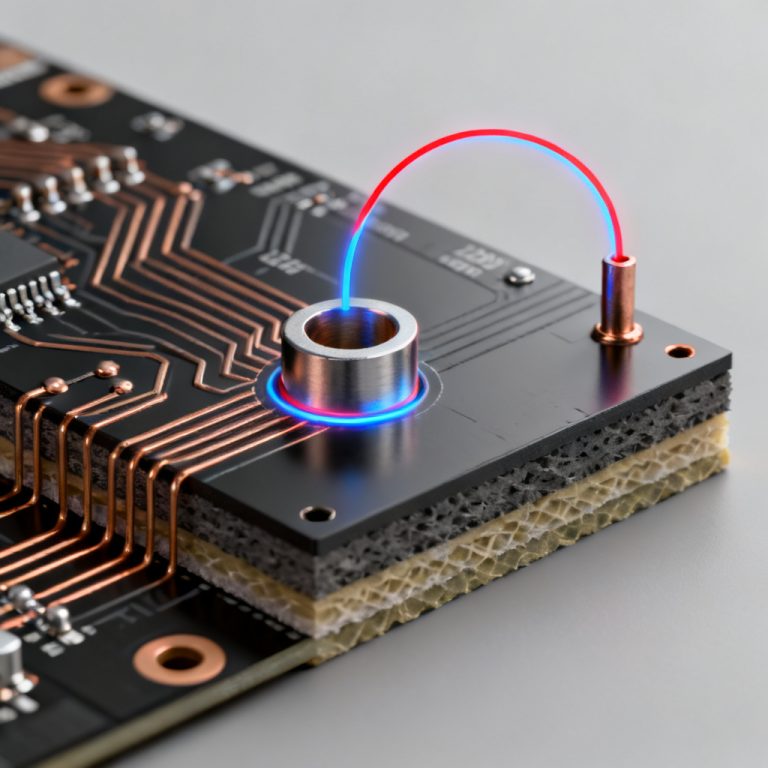
7.2 Crosstalk and Return Path Discontinuities in High Speed PCB
A split plane or missing via stitching can dramatically increase crosstalk. 3D solvers are essential for modeling these effects. A 2D solver assumes an ideal return path, while a 3D solver shows true coupling.
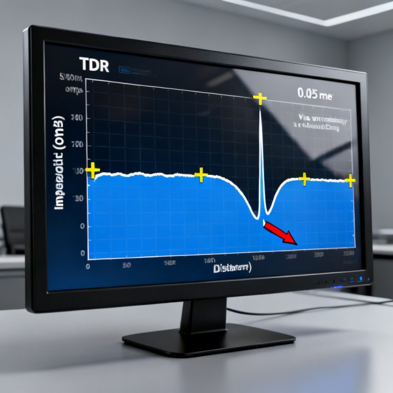
7.3 Time-Domain vs. Frequency-Domain Analysis for High Speed PCB
In frequency domain, use S-parameters to see crosstalk peaks at specific frequencies. In time domain, use TDR/TDT to see crosstalk pulse shapes and delays. 3D solvers can export time-domain results directly.
7.4 Correlation with Measurement for High Speed PCB
Always correlate simulation results with lab measurements using VNA or TDR. 2D solvers often match well for simple structures; 3D solvers are needed for complex geometries to achieve less than 1 dB correlation.
FAQ: Crosstalk in High Speed PCB Field Solver Setup
What is the best field solver for crosstalk in high-speed PCB design?
The best solver depends on your design stage. 2D solvers are ideal for pre-layout rules, 2.5D solvers for post-layout verification, and 3D solvers for final sign-off on complex structures.
Can a 2D solver accurately predict crosstalk in high-speed PCB?
Yes, for long, uniform traces, 2D solvers provide highly accurate RLCG matrices. However, they cannot model discontinuities like vias or bends.
When should I use a 3D solver for high-speed PCB crosstalk?
Use 3D solvers for ultra-high-speed designs above 56 Gbps, connectors, BGA packages, or when modeling crosstalk through multiple vias and layers.
What parameters are essential for crosstalk analysis in high-speed PCB?
Essential parameters include mutual inductance (L12), mutual capacitance (C12), characteristic impedance (Z0), propagation delay (Tpd), and coupling coefficient (K).
Conclusion: Making the Right Choice for Your High-Speed PCB
Crosstalk analysis is not a one-size-fits-all task. The choice between 2D, 2.5D, and 3D field solvers depends on your design stage, complexity, and accuracy requirements. Start with 2D for design rules and feasibility. Move to 2.5D for layout validation and S-parameter extraction. Reserve 3D for final sign-off and complex structures. By understanding the strengths and limitations of each solver type, you can achieve accurate crosstalk predictions without wasting simulation time. For our high-speed PCB manufacturing and assembly services, we recommend using a combination of all three methods to ensure your design meets signal integrity targets from concept to production. Need help with your high-speed PCB design? Contact our engineering team for a free crosstalk analysis consultation. We specialize in manufacturing PCBs with controlled impedance, tight coupling tolerances, and optimized stackups for data rates up to 112 Gbps.
This pillar page was compiled from expert sources including Altium Academy, Cadence Sigrity, and Sierra Circuits technical documentation. All non-redundant, actionable insights have been preserved to provide the most comprehensive guide available.