In high-speed PCB design, differential pair crosstalk is a critical signal integrity challenge that engineers must master. This comprehensive guide explores the two fundamental types of coupling—intra-pair and inter-pair—providing actionable strategies to optimize your high-speed PCB layouts for reliable performance at multi-gigabit data rates.
Understanding Differential Pairs in High Speed PCB
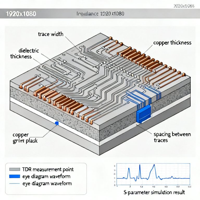
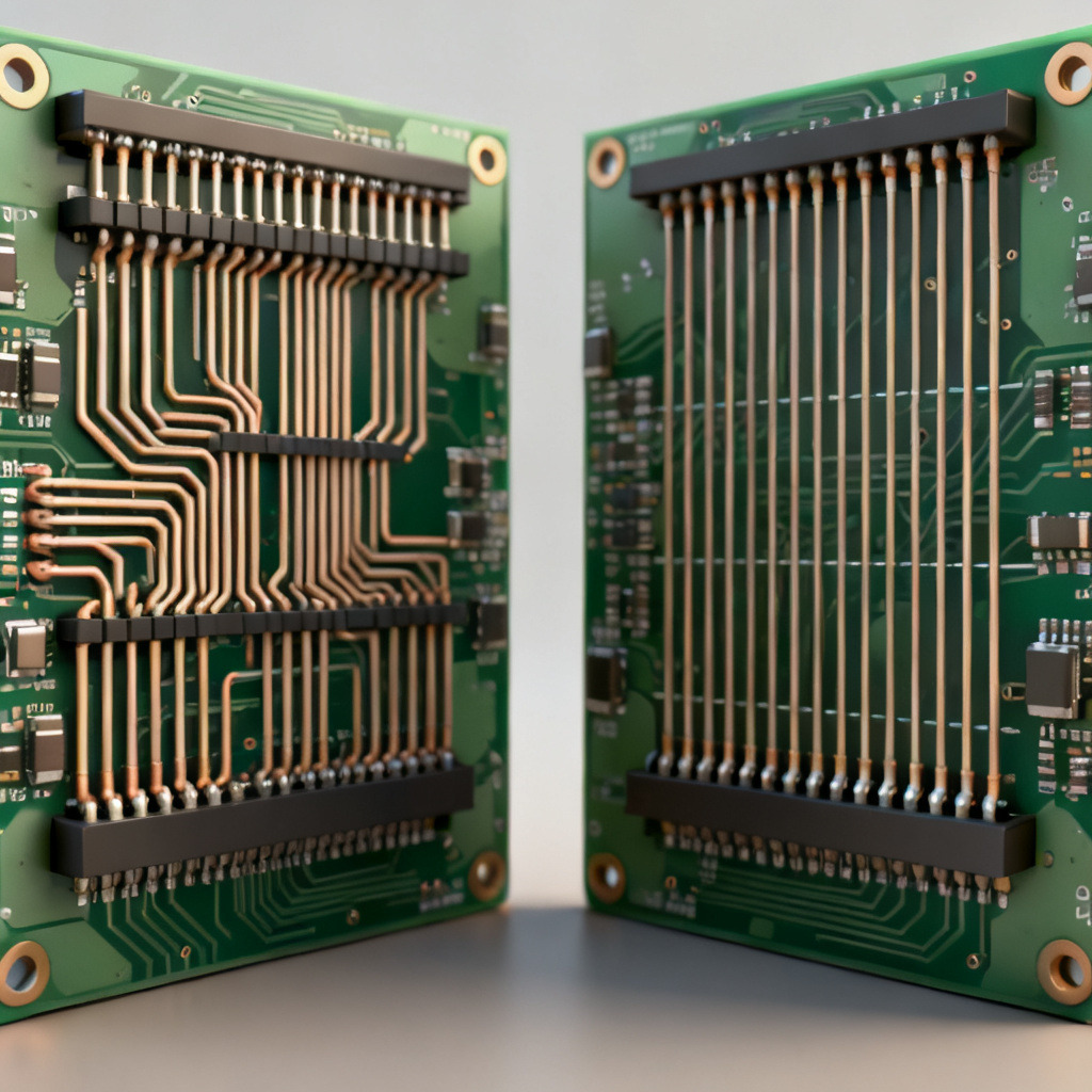
A differential pair in high-speed PCB design consists of two complementary traces carrying equal and opposite signals. This configuration offers superior noise immunity, reduced EMI, and lower voltage swings compared to single-ended signaling. Key parameters include differential impedance (Z_diff), common-mode impedance (Z_common), odd-mode impedance (Z_odd), and even-mode impedance (Z_even).
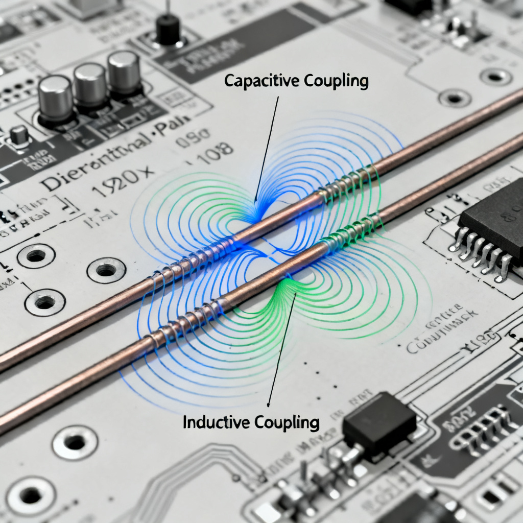
The physics of coupling in differential pairs involves both capacitive (C_m) and inductive (L_m) components. The coupling coefficient (k) is defined as k = (Z_even – Z_odd) / (Z_even + Z_odd). For tightly coupled pairs, k ranges from 0.2 to 0.4, while loosely coupled pairs have k below 0.1.
Intra-Pair Coupling in High Speed PCB: Internal Dynamics
Intra-pair coupling refers to the electromagnetic interaction between the two traces within a single differential pair. This intentional coupling is fundamental to differential signaling and directly determines the pair’s impedance characteristics.
Key Effects of Intra-Pair Coupling
Intra-pair coupling directly influences impedance control, skew timing, and mode conversion. Tight coupling (small trace spacing) increases mutual capacitance and inductance, lowering Z_diff. Loose coupling increases Z_diff. If traces are asymmetrical, intra-pair coupling can cause differential-to-common-mode conversion, leading to timing errors.
Mitigation Strategies for Intra-Pair Coupling
- Maintain constant spacing between traces
- Use symmetrical routing with identical trace lengths
- Optimize trace width and dielectric height using 2D field solvers
- Avoid 90-degree bends; use 45-degree or chamfered bends
- Manage vias symmetrically to preserve impedance
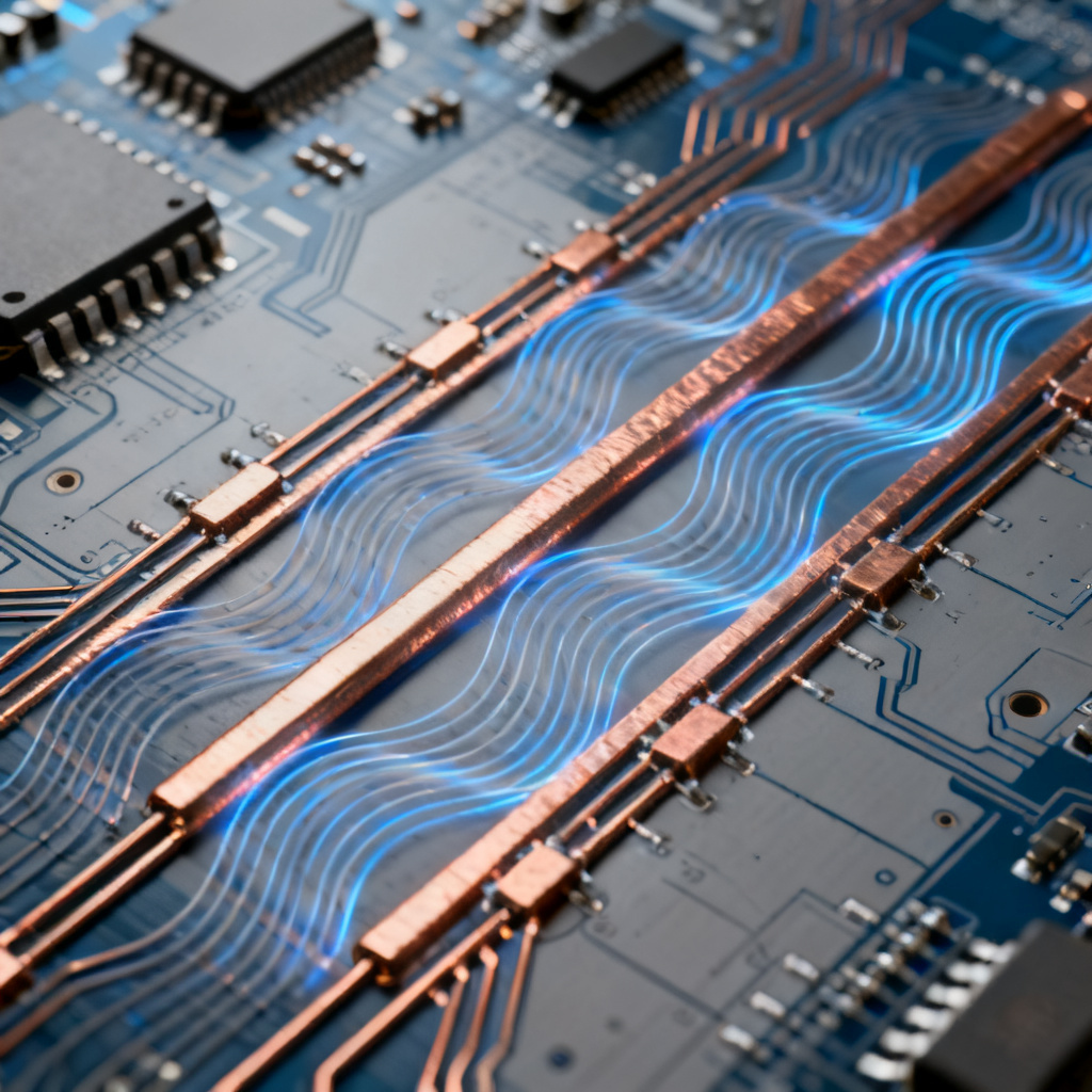
Inter-Pair Coupling in High Speed PCB: The External Threat
Inter-pair coupling, also known as alien crosstalk, occurs between adjacent differential pairs. Unlike intra-pair coupling, this is a parasitic effect that degrades signal integrity and must be minimized.
Types of Inter-Pair Coupling
Near-End Crosstalk (NEXT) appears at the same end as the aggressor driver, while Far-End Crosstalk (FEXT) appears at the opposite end. FEXT is particularly problematic in high-speed serial links.
Key Factors Influencing Inter-Pair Coupling
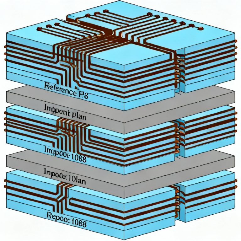
The primary variable is distance between pairs (D). A closer reference plane reduces fringe fields. Wider traces and thicker dielectrics increase coupling. High-density routing exacerbates the problem.
Mitigation Strategies for Inter-Pair Coupling
- Increase inter-pair spacing (use 3W rule as baseline, 5W for 25+ Gbps)
- Use staggered routing to reduce cumulative coupling
- Insert guard traces (though effectiveness decreases at high frequencies)
- Use differential stripline for better shielding
- Avoid long parallel routing; limit to under 1 inch
- Place ground vias around differential vias
Intra-Pair vs Inter-Pair Coupling: Comparative Analysis
Understanding the differences between intra-pair and inter-pair coupling is essential for optimizing high-speed PCB designs.
| Aspect | Intra-Pair Coupling | Inter-Pair Coupling |
|---|---|---|
| Nature | Intentional (design feature) | Parasitic (unwanted) |
| Impact on Impedance | Directly determines Z_diff | Minimal direct impact |
| Frequency Dependence | Strong at all frequencies | Increases with frequency |
| Mitigation Difficulty | Easy; controlled by geometry | Challenging; layout trade-offs |
| Typical Magnitude | High (k = 0.2–0.4) | Low (k < 0.1) |
| Measurement | TDR | TDR or VNA |
A common design dilemma: tight coupling reduces inter-pair crosstalk but increases manufacturing sensitivity. For most high-speed PCB designs, moderately tight coupling (S/H ratio of 0.5–1.0) provides the best balance. Always verify with 3D electromagnetic simulations for critical nets.
Simulation and Measurement Techniques for Differential Pair Crosstalk
Accurate simulation is crucial for managing differential pair crosstalk in high-speed PCBs.
Simulation Tools
- 2D Field Solvers (Polar Si9000, Saturn PCB Toolkit) for quick impedance calculations
- 3D EM Solvers (Ansys HFSS, CST Studio Suite) for accurate crosstalk modeling
- IBIS-AMI Models for system-level analysis
Key Metrics
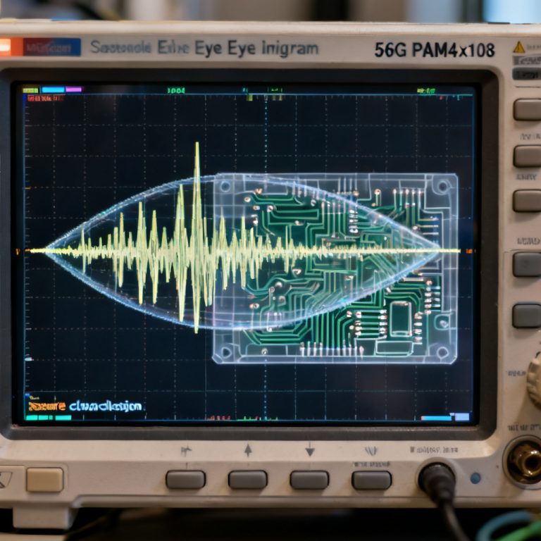
Extract S-parameters (S11, S21, S31, S41), TDR impedance profiles, and eye diagrams to evaluate voltage margin and jitter.
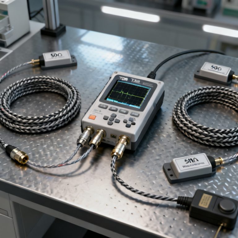
Measurement Best Practices
- Use differential probes with matched impedance
- Calibrate to the DUT plane using SOLT
- Measure both NEXT and FEXT
- Correlate measurements with simulations
Advanced Topics in Differential Pair Crosstalk
In multilayer PCBs, differential pairs on different layers can couple through plane resonance. Use multiple ground vias to stitch planes together. In flexible PCBs, intra-pair coupling is often weaker due to larger S/H ratios. AI-driven optimization tools like Cadence Allegro AI can automatically adjust spacing. In advanced packaging (FCBGA), fine pitch requires tight intra-pair control.
Practical Design Guidelines for High Speed PCB
Checklist for Differential Pair Routing
- Define target impedance (typically 100Ω)
- Calculate geometry using 2D field solver
- Maintain symmetry (equal length ±5 mils)
- Minimize skew within 1% of wavelength
- Control inter-pair spacing (D ≥ 3W microstrip, D ≥ 2W stripline)
- Add ground vias every λ/10
- Simulate critical nets above 10 Gbps
- Account for ±10% etching variation
Common Mistakes to Avoid
- Ignoring intra-pair skew (1 ps causes 3 dB noise at 10 GHz)
- Over-tight coupling (S < 2W increases manufacturing risk)
- Routing through dense via fields
- Neglecting return path integrity
Frequently Asked Questions
What is the difference between intra-pair and inter-pair crosstalk in high-speed PCB?
Intra-pair crosstalk occurs between the two traces within a single differential pair and is intentional for impedance control. Inter-pair crosstalk occurs between adjacent differential pairs and is a parasitic effect that degrades signal integrity.
How can I reduce differential pair crosstalk in my PCB design?
To reduce differential pair crosstalk, increase inter-pair spacing (use 3W rule), use differential stripline layers, add guard traces, and maintain symmetrical routing for intra-pair coupling.
What is the recommended spacing for differential pairs to minimize crosstalk?
For microstrip, maintain at least 3× the trace width (3W) between pairs. For stripline, 2W may suffice. For very high-speed designs (25+ Gbps), use 5W or more and verify with simulations.
Does tight intra-pair coupling help reduce inter-pair crosstalk?
Yes, tight intra-pair coupling confines fields between the two traces, reducing fringe fields that cause inter-pair coupling. However, it increases sensitivity to manufacturing tolerances.