In modern high-frequency and high-speed digital designs, Impedance Control PCB for Coplanar Waveguide is essential for signal integrity. This page compares grounded (GCPW) and ungrounded (CPW) configurations to help you choose the optimal transmission line for your next RF or high-speed project.
1. Fundamentals of Impedance Control PCB for Coplanar Waveguide
1.1 What is a Coplanar Waveguide?
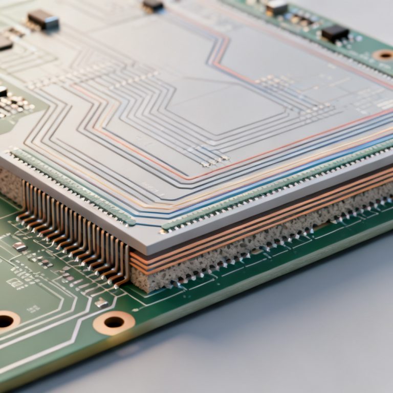
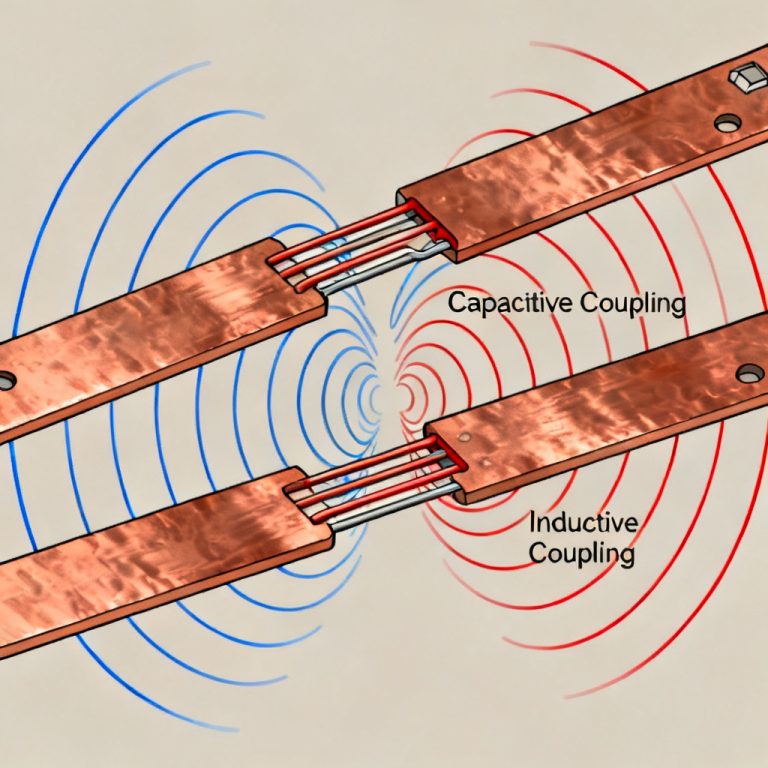
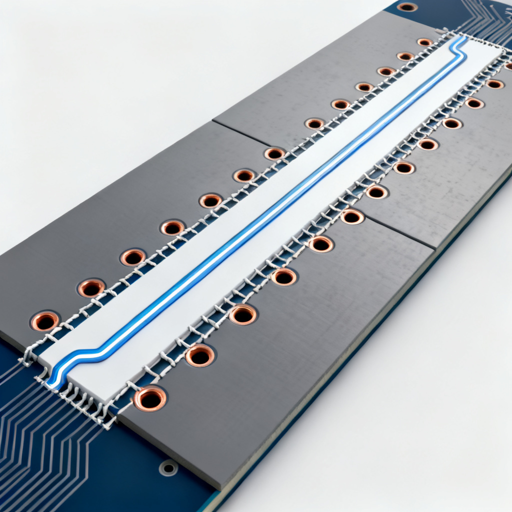
A coplanar waveguide for Impedance Control PCB consists of a center signal trace with two ground planes on the same layer, separated by a uniform gap. Unlike microstrip, all conductors are on the top copper layer, supporting a quasi-TEM mode from DC to millimeter-wave.
1.2 Key Parameters for Impedance Control PCB
| Parameter | Description | Impact on Impedance Control PCB |
|---|---|---|
| Trace width (W) | Width of center signal conductor | Directly determines characteristic impedance (Z₀) with gap |
| Gap (G) | Spacing between signal and ground planes | Critical for impedance accuracy in coplanar waveguide |
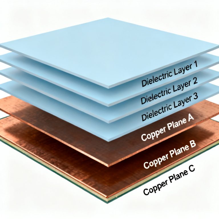
| Substrate height (H) | Dielectric thickness between top copper and any internal ground plane | Modulates impedance, especially in grounded CPW |
| Dielectric constant (εᵣ) | Material property affecting wave propagation | Affects effective permittivity and impedance |
| Copper thickness (T) | Thickness of copper foil | Shifts impedance, especially for thin substrates |
1.3 Why Choose CPW for Impedance Control PCB?
In Impedance Control PCB design, CPW offers no via stitching for ground connection, low dispersion at high frequencies, easier component mounting with ground on the same layer, and better isolation between adjacent traces.
2. Ungrounded CPW – Design & Characteristics for Impedance Control PCB
2.1 Structure
Ungrounded CPW has no continuous ground plane on the bottom layer, making it a single-layer transmission line suitable for cost-sensitive Impedance Control PCB designs.
2.2 Impedance Control for Ungrounded CPW
Impedance is primarily a function of W/G ratio and εᵣ. For a 50Ω Impedance Control PCB on FR4 (εᵣ=4.5, H=1.6mm), typical values are W≈0.5mm with G≈0.25mm. The approximate formula is Z₀ ≈ (60/√εᵣ) * ln(1.9 * (2W+G)/(0.8W+G)).
2.3 Advantages
No backside metallization required, lower parasitic capacitance, and easier 2D modeling.
2.4 Disadvantages
Higher radiation loss above 10 GHz, susceptibility to parasitic modes on thick substrates, and poor heat dissipation.
2.5 When to Use Ungrounded CPW
Frequencies below 10 GHz, low-cost low-layer-count designs, high-impedance applications, and prototyping where via stitching is impractical.
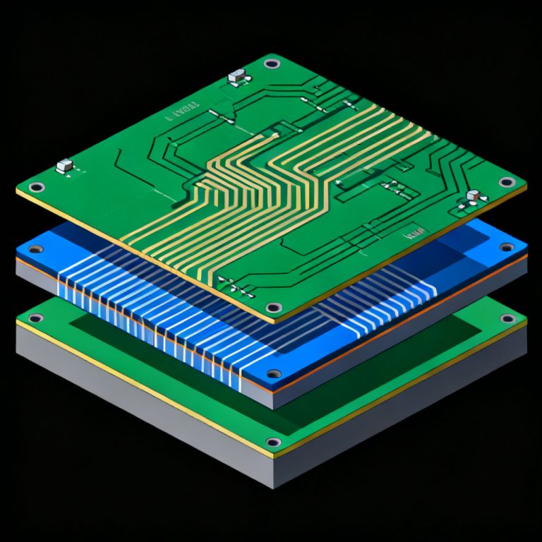
3. Grounded CPW (GCPW) – Design & Characteristics for Impedance Control PCB
3.1 Structure
GCPW adds a continuous bottom ground plane connected to top grounds via stitching vias, creating a shielded Impedance Control PCB structure that suppresses parasitic modes and reduces radiation.
3.2 Impedance Control for GCPW
Impedance depends on W, G, H, εᵣ, and T. The bottom ground plane lowers effective impedance, so for the same target Z₀, W/G must be adjusted (narrower trace or larger gap) compared to ungrounded CPW. The ratio H/(W+2G) must exceed 1 to avoid significant impedance shift.
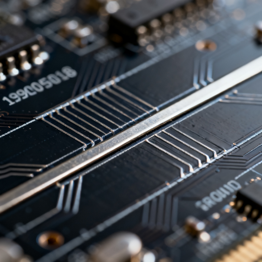
3.3 Via Stitching Rules for Impedance Control PCB
| Parameter | Requirement | Impact on Impedance Control PCB |
|---|---|---|
| Via spacing (S_via) | ≤ λ/20 at highest frequency | Prevents slotline mode and maintains impedance accuracy |
| Via diameter | 0.2–0.3 mm typical | Ensures low inductance ground connection |
| Placement | Close to gap edge (within 2× gap width) | Minimizes parasitic inductance |
3.4 Advantages
Superior isolation, lower radiation loss essential for millimeter-wave, better heat sinking, and higher power handling.
3.5 Disadvantages
Higher fabrication cost, potential resonant modes if via spacing is too large, and more complex 3D modeling.
3.6 When to Use GCPW
Frequencies above 10 GHz (especially above 20 GHz), high-density RF modules, low-EMI designs, and tight impedance tolerance (±5% or better).
4. Comparison: Grounded vs Ungrounded CPW for Impedance Control PCB
| Parameter | Ungrounded CPW | Grounded CPW (GCPW) |
|---|---|---|
| Impedance range | 30–200Ω | 20–120Ω |
| Loss (at 10 GHz) | ~0.5 dB/cm (FR4) | ~0.3 dB/cm (FR4) |
| Radiation loss | Moderate | Low |
| Via complexity | None | Required (stitching) |
| Manufacturing cost | Low | Moderate |
| Max frequency | <20 GHz | >60 GHz |
| Thermal performance | Poor | Good |
5. Practical Design Guidelines for Impedance Control PCB
5.1 Material Selection
For GCPW above 20 GHz, use low-loss materials like Rogers 4350B or Isola Astra MT77. For ungrounded CPW, standard FR4 is acceptable up to 6 GHz with careful impedance control. Specify ±2% εᵣ tolerance.
5.2 Impedance Calculation Tools
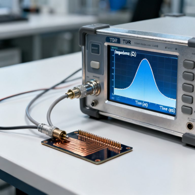
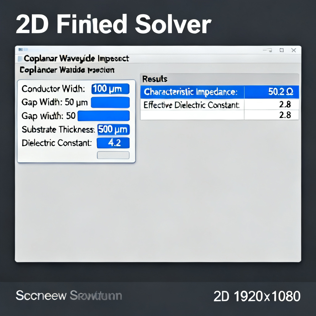
Use 2D field solvers like Polar Si9000 or Ansys Q3D for accurate Impedance Control PCB design. For initial estimates, use online calculators from Microwaves101 or Altium. Always include copper thickness in calculations.
5.3 Transition Design
Use tapered transitions (linear or Klopfenstein) to minimize reflections. For GCPW to microstrip, remove the bottom ground plane under the microstrip section. Keep transition length greater than 3× trace width for return loss below -20 dB.
5.4 Ground Plane Integrity
In GCPW, ensure the bottom ground plane extends at least 5× trace width beyond the gap. Avoid slots or cutouts under the CPW trace. For ungrounded CPW, consider a floating ground plane on a lower layer to reduce radiation.
5.5 Manufacturing Tolerances
Etching tolerance of ±0.025mm for controlled impedance lines. Dielectric thickness tolerance of ±10% for FR4, ±5% for high-frequency laminates. Ensure via registration is centered within the ground pad.
6. Common Pitfalls in Impedance Control PCB Design
6.1 Slotline Mode in GCPW
If via spacing exceeds λ/20, the two ground planes can resonate, creating a slotline mode. Use via spacing ≤ λ/20; for 28 GHz, this is less than 0.5mm in FR4.
6.2 Impedance Mismatch Due to Copper Thickness
Thick copper (2oz+) narrows the effective gap, lowering impedance. Adjust W and G in the design tool to account for copper thickness.
6.3 Ground Plane Discontinuity at Connectors
SMA or edge-launch connectors often have a ground plane cutout that disrupts GCPW. Use connector footprints designed for CPW and add ground vias around the connector launch.
6.4 Substrate Mode Excitation in Ungrounded CPW
Thick substrate (H > λ/10) can support parallel-plate modes. Use thin substrate (e.g., 0.254mm Rogers for >30 GHz) or switch to GCPW.
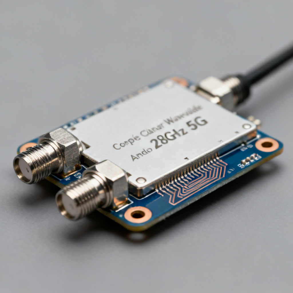
7. Case Study: 28 GHz 5G Antenna Feed for Impedance Control PCB
Requirement: 50Ω impedance, less than 0.5 dB insertion loss, low radiation. Design choice: GCPW on Rogers 4350B (εᵣ=3.48, H=0.254mm, 1oz copper). W=0.3mm, G=0.2mm from field solver. Via spacing=0.3mm (λ/20 at 28 GHz ≈ 0.45mm). Transition to microstrip for antenna patch: 4mm tapered section. Result: Measured Z₀=49.8Ω, insertion loss=0.4 dB at 28 GHz, return loss below -25 dB.
8. Conclusion: Which CPW for Your Impedance Control PCB?
Ungrounded CPW is ideal for low-cost, low-frequency (<10 GHz) designs where simplicity and high impedance are needed. Grounded CPW (GCPW) is the industry standard for high-performance RF, microwave, and millimeter-wave Impedance Control PCB applications, offering superior loss, isolation, and thermal management. For most B2B PCB procurement scenarios, GCPW is the recommended choice. Always consult with your PCB manufacturer early to verify stackup, material availability, and via capabilities.
FAQ: Impedance Control PCB for Coplanar Waveguide
What is the difference between grounded and ungrounded coplanar waveguide for impedance control PCB?
In an Impedance Control PCB, grounded coplanar waveguide (GCPW) includes a bottom ground plane with stitching vias, reducing radiation and improving isolation. Ungrounded CPW lacks this plane, offering lower cost but higher loss at high frequencies.
How do I calculate impedance for a coplanar waveguide PCB?
Use 2D field solvers like Polar Si9000 or online calculators from Microwaves101. For Impedance Control PCB design, include trace width, gap, substrate height, dielectric constant, and copper thickness.
When should I use grounded CPW instead of ungrounded CPW?
Use grounded CPW for frequencies above 10 GHz, tight impedance tolerance, low EMI requirements, and millimeter-wave applications. Ungrounded CPW suits lower frequencies and cost-sensitive Impedance Control PCB projects.
What is the role of via stitching in grounded CPW?
Via stitching connects top ground planes to the bottom ground plane, suppressing slotline modes and ensuring consistent impedance in an Impedance Control PCB. Spacing must be ≤ λ/20.
Can I use FR4 for high-frequency coplanar waveguide PCBs?
FR4 is acceptable up to 6 GHz for ungrounded CPW with careful impedance control. For higher frequencies, use low-loss materials like Rogers to maintain Impedance Control PCB performance.
“`