[rank_math_breadcrumb]
Mastering Differential Pair Impedance for PCIe 5.0 is critical for high-speed PCB design at 32 GT/s. This guide explains the 85Ω vs 100Ω standard, why 85Ω is required, and how to verify impedance through TDR, VNA, and simulation.
1. The Fundamental Difference: 85Ω vs 100Ω for PCIe 5.0
1.1 PCI-SIG Standard for PCIe 5.0 Differential Pair Impedance
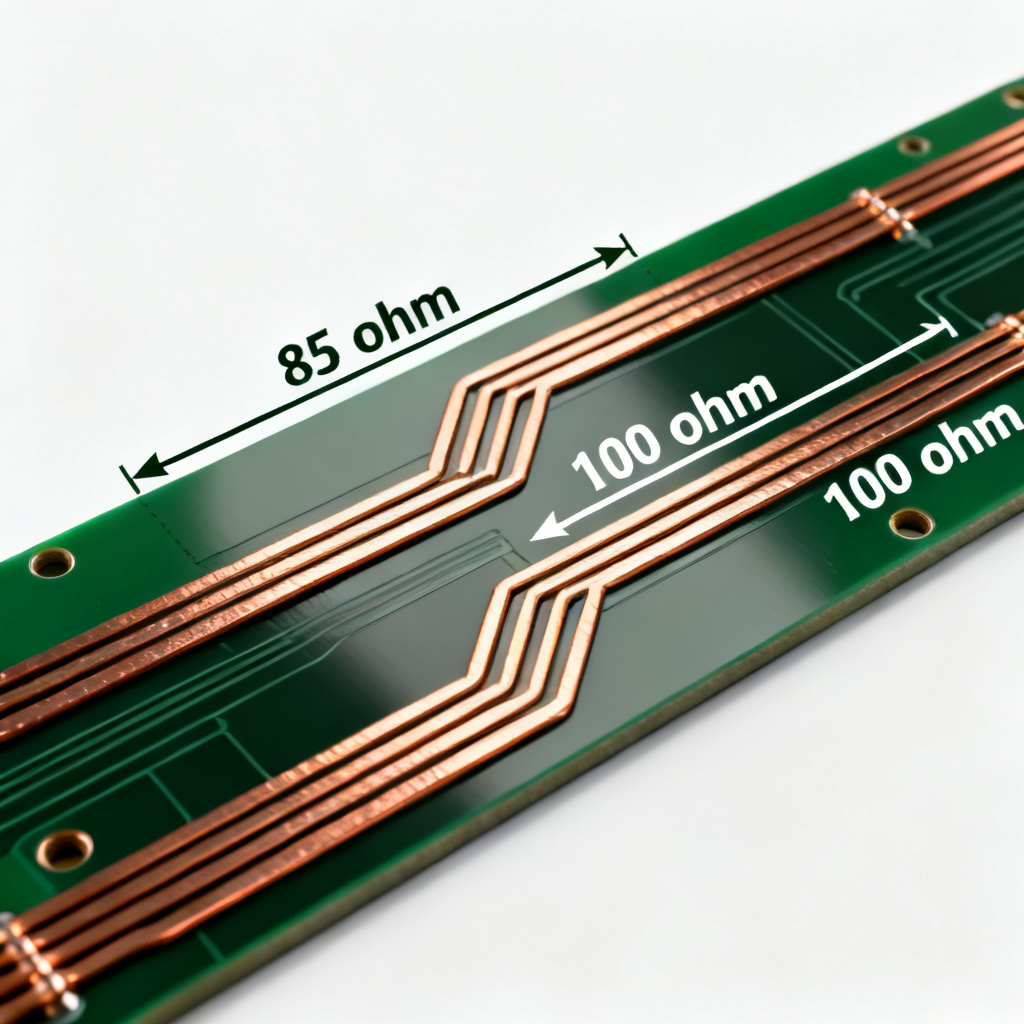
According to the PCI Express Base Specification Revision 5.0, Version 1.0, the Differential Pair Impedance for PCIe 5.0 must be 85Ω ± 15% (72.25Ω to 97.75Ω). This is a mandatory departure from earlier PCIe generations (1.0 through 3.0) which commonly used 100Ω differential impedance. For PCIe 4.0, the specification also moved toward 85Ω, but PCIe 5.0 solidifies this as the mandatory target for all new designs.
Why 85Ω? The shift to 85Ω is driven by signal integrity at 32 GT/s. Higher data rates require lower impedance to reduce reflections, crosstalk, and insertion loss. A lower impedance (85Ω vs 100Ω) provides better signal integrity by:
- Reducing voltage swing: Lower impedance lowers the voltage swing, which reduces power consumption and electromagnetic interference (EMI).
- Improving impedance matching: Many PCB materials (e.g., low-loss laminates like Megtron 6 or IS620) have a natural characteristic impedance closer to 85Ω when designed with standard trace widths and stackups. Forcing 100Ω often requires narrower traces or wider spacing, which can increase losses.
- Compatibility with connectors and packages: PCIe 5.0 connectors and chip packages are designed for 85Ω. Using 100Ω can cause impedance mismatches at these interfaces, leading to signal degradation.
1.2 When 100Ω Still Applies for Differential Pair Impedance
Despite the 85Ω standard for PCIe 5.0, 100Ω differential impedance is still relevant in specific scenarios:
- Legacy PCIe designs: For PCIe 3.0 or earlier, 100Ω remains the standard.
- Other high-speed interfaces: Protocols like USB 3.0/3.1, SATA, and DisplayPort often require 100Ω. If your board combines PCIe 5.0 with these interfaces, you may need to maintain 100Ω for those lanes.
- Custom or non-compliant designs: Some proprietary systems or older chipsets may still use 100Ω, but this is rare for PCIe 5.0.
Key Takeaway: For PCIe 5.0, always target 85Ω differential impedance. Never assume 100Ω unless you have explicit verification from the chipset or connector manufacturer.
2. How Differential Pair Impedance Affects Signal Integrity at 32 GT/s
2.1 The Physics of High-Speed Transmission
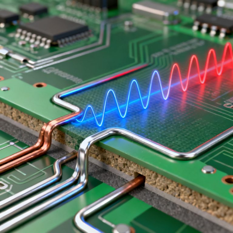
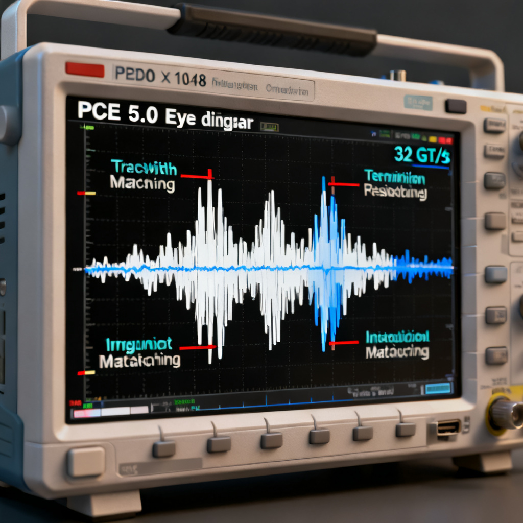
At 32 GT/s, the signal rise time is extremely fast (typically < 20 ps). This makes the transmission line behave as a distributed network rather than a simple wire. Any impedance discontinuity—whether from a via, connector, or trace width change—will cause a reflection. Reflections can lead to:
- Jitter: Timing errors that degrade the eye diagram.
- Insertion loss: Signal amplitude reduction due to reflections and dielectric losses.
- Crosstalk: Unwanted coupling between adjacent traces.
2.2 Why 85Ω is Superior for PCIe 5.0 Signal Integrity
Research and simulations by leading PCB manufacturers and signal integrity engineers consistently show that 85Ω differential impedance offers:
- Lower insertion loss: At 16 GHz (the Nyquist frequency for 32 GT/s), 85Ω traces exhibit approximately 0.5 dB less loss per inch compared to 100Ω traces, due to wider trace widths.
- Better eye diagram margins: The eye opening (both vertical and horizontal) is larger with 85Ω, providing more tolerance to process variations and temperature changes.
- Reduced crosstalk: The wider trace width (for 85Ω) increases spacing between pairs, reducing coupling.
2.3 The Role of PCB Material in Differential Pair Impedance
The choice of PCB laminate is critical. For PCIe 5.0, materials with a low dissipation factor (Df < 0.005 at 10 GHz) are recommended, such as:
- Rogers 4350B
- Isola I-Speed
- Panasonic Megtron 6
- Taconic RF-35
These materials maintain stable impedance across frequency and temperature. Standard FR-4 (Df ~0.02) will cause excessive loss and impedance variation, making it unsuitable for PCIe 5.0.
3. How to Verify Differential Pair Impedance for PCIe 5.0
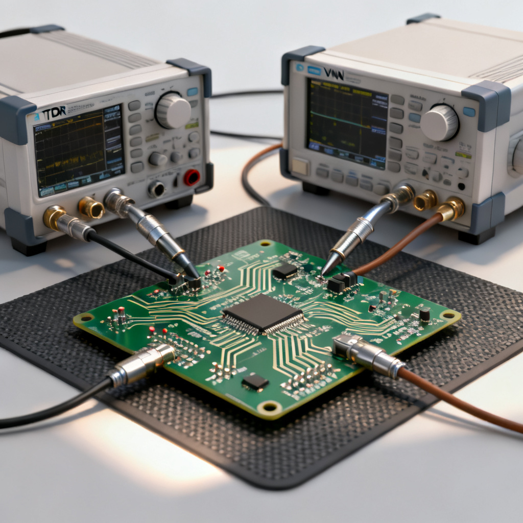
3.1 Pre-Production: Simulation with 2D Field Solvers
Before manufacturing, use a 2D field solver (e.g., Polar SI9000, Simbeor, or Ansys Q2D) to calculate the trace geometry needed for 85Ω differential impedance. Input parameters include:
- Dielectric constant (Dk): Use the manufacturer’s value at your operating frequency (e.g., 3.5 for Megtron 6 at 10 GHz).
- Dielectric thickness: The distance from the trace to the reference plane.
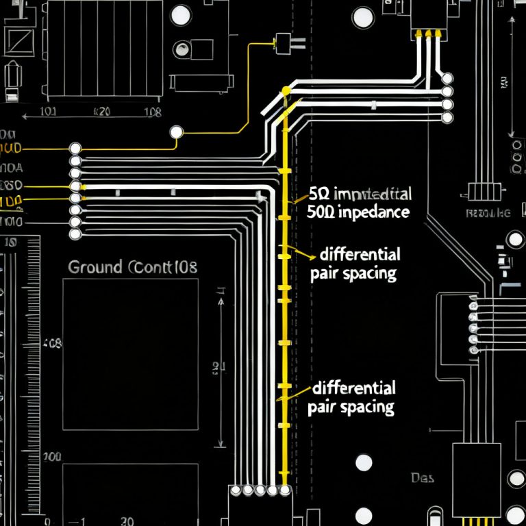
- Trace width and spacing: For 85Ω, typical values are 4-5 mil width with 5-6 mil spacing, but this varies with stackup.
- Copper thickness: 0.5 oz or 1 oz is standard; thicker copper increases impedance.
Simulation Steps:
- Define the stackup with layer thicknesses and material Dk/Df.
- Set the target impedance to 85Ω differential.
- Run the solver to find the optimal trace width and spacing.
- Perform a parametric sweep to account for manufacturing tolerances (e.g., ±10% etch variation).
3.2 Post-Production: TDR (Time Domain Reflectometry)
TDR is the most common method for verifying differential impedance on a fabricated PCB. A TDR sends a fast step pulse (rise time < 35 ps for PCIe 5.0) down the trace and measures the reflected signal. The impedance is calculated from the reflection coefficient.
How to Perform TDR Testing:
- Use a differential TDR probe: Connect to the differential pair at the connector or test point.
- Calibrate the instrument: Use a known 50Ω reference (for single-ended) or 100Ω reference (for differential).
- Measure the impedance profile: The TDR displays impedance vs. distance. Look for:
- Average impedance: Should be 85Ω ± 15% (72.25Ω to 97.75Ω).
- Impedance variations: Spikes or dips indicate discontinuities (e.g., vias, stubs, or etch errors).
- Ringing: Excessive ringing suggests poor termination or mismatched connectors.
- Key metrics:
- Impedance at launch point: Typically 100Ω (from the probe), but the trace should settle to 85Ω.
- Impedance at the end: If open, expect a rise to > 200Ω; if terminated with 85Ω, it should stay flat.
3.3 Post-Production: VNA (Vector Network Analyzer)
For rigorous validation, especially at high frequencies, a VNA measures S-parameters (scattering parameters) to characterize impedance and insertion loss. This is more accurate than TDR for frequency-dependent effects.
How to Perform VNA Testing:
- Use a differential VNA or single-ended VNA with a balun: Convert to differential mode.
- Calibrate with SOLT (Short-Open-Load-Thru) standards: Up to 20 GHz or higher.
- Measure Sdd21 (differential insertion loss): Ensure it is below -3 dB at 16 GHz (for 32 GT/s).
- Extract impedance from S-parameters: The differential impedance Zdiff can be calculated from the reflection coefficient Sdd11. A flat Sdd11 below -20 dB indicates good impedance matching.
- Frequency sweep: Check impedance stability from DC to 20 GHz. If impedance varies significantly with frequency, your material Dk is likely dispersive (common with FR-4).
3.4 In-System Verification: Eye Diagram Testing
The ultimate test is whether the PCIe 5.0 link works reliably. Use an oscilloscope with a differential probe to capture the eye diagram at the receiver.
- Eye height: Should exceed 50 mV (typical for PCIe 5.0).
- Eye width: Should exceed 0.3 UI (Unit Interval), where UI = 31.25 ps.
- Jitter: Total jitter (TJ) should be less than 0.2 UI.
If the eye diagram is closed or marginal, check impedance with TDR/VNA to identify the root cause.
4. Common Mistakes in Differential Pair Impedance for PCIe 5.0
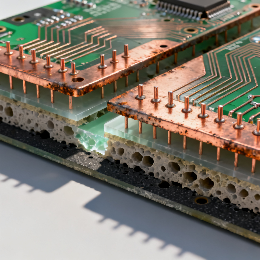
4.1 Ignoring the Reference Plane
Following differential pair routing rules: Differential impedance is highly dependent on the reference plane. If the plane is cut or has large gaps (e.g., for vias or split planes), impedance will shift. Always ensure a continuous ground plane under differential pairs.
4.2 Using the Wrong Material Dk
Dk varies with frequency and temperature. Using a Dk value from a datasheet at 1 GHz for a 16 GHz design will result in incorrect impedance. Always use the Dk at your operating frequency (16 GHz for PCIe 5.0).
4.3 Neglecting Via Stubs
Vias create impedance discontinuities. For PCIe 5.0, use back-drilled vias or microvias to minimize stub length. A stub longer than 10 mils can cause significant reflection.
4.4 Assuming 100Ω is Safe
Some designers default to 100Ω because it was standard for PCIe 3.0. This is a critical error. Always verify the PCIe generation requirement with your chipset vendor.
5. Practical Design Guidelines for 85Ω Differential Pairs
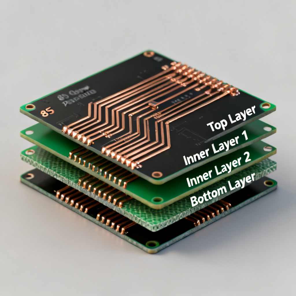
To achieve reliable 85Ω impedance, follow these guidelines:
- Trace width: 4-5 mils (depending on stackup).
- Trace spacing: 5-6 mils (edge-to-edge).
- Dielectric thickness: 3-5 mils between the trace layer and reference plane.
- Copper weight: 0.5 oz (1.4 mils) for lower loss.
- Length matching: Match lengths within 5 mils for differential pairs.
- Avoid 90-degree bends: Use 45-degree chamfered bends or curved traces.
- Stitch vias: Place ground vias every 100 mils along the pair to reduce crosstalk.
Example Stackup for 85Ω (6-layer board)
| Layer | Type | Trace Width (mil) | Spacing (mil) | Dielectric Thickness (mil) | Dk at 10 GHz |
|---|---|---|---|---|---|
| Layer 1 (Top) | Signal (Differential pairs) | 4.5 | 5.5 | 3.5 | 3.5 |
| Layer 2 | Ground plane | – | – | – | – |
| Layer 3 | Power plane | – | – | – | – |
| Layer 4 | Signal (Differential pairs) | 4.5 | 5.5 | 3.5 | 3.5 |
| Layer 5 | Ground plane | – | – | – | – |
| Layer 6 | Bottom signal | – | – | – | – |
6. FAQ: Differential Pair Impedance for PCIe 5.0
What is the standard differential pair impedance for PCIe 5.0?
The standard Differential Pair Impedance for PCIe 5.0 is 85Ω ± 15%, as defined by the PCI-SIG specification.
Why is 85Ω used instead of 100Ω for PCIe 5.0?
85Ω is used to improve signal integrity at 32 GT/s, reducing insertion loss, reflections, and crosstalk compared to 100Ω.
Can I use 100Ω for PCIe 5.0 if my design is legacy?
No. PCIe 5.0 requires 85Ω. Using 100Ω will cause impedance mismatches and signal degradation. Always follow the PCI-SIG standard.
How do I verify differential pair impedance on a fabricated PCB?
Use TDR (Time Domain Reflectometry) for a quick impedance profile, or VNA (Vector Network Analyzer) for frequency-domain validation. Simulation with tools like Polar SI9000 is recommended before fabrication.
What PCB materials are best for PCIe 5.0 impedance control?
Low-loss materials such as Rogers 4350B, Isola I-Speed, Panasonic Megtron 6, or Taconic RF-35 with Df < 0.005 at 10 GHz are recommended.
7. Glossary of Key Terms
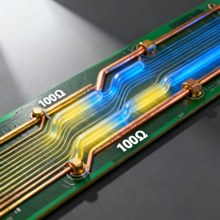
- Differential Pair Impedance: The impedance between two coupled traces carrying equal and opposite signals, critical for high-speed interfaces like PCIe 5.0.
- PCIe 5.0: The fifth generation of PCI Express, operating at 32 GT/s per lane.
- TDR (Time Domain Reflectometry): A measurement technique that sends a fast pulse to detect impedance changes along a transmission line.
- VNA (Vector Network Analyzer): An instrument that measures S-parameters to characterize high-frequency behavior, including impedance and insertion loss.
- Insertion Loss: The loss of signal power resulting from the insertion of a device or transmission line in a system.
- Eye Diagram: A graphical representation of a digital signal’s quality, showing voltage and timing margins.
8. Comparison: 85Ω vs 100Ω for High-Speed PCB Design
For PCIe 5.0, 85Ω differential impedance is the clear winner due to lower insertion loss, better eye diagram margins, and reduced crosstalk. While 100Ω remains relevant for legacy PCIe generations and other protocols (USB 3.0, SATA), it is not compliant with PCIe 5.0 specifications. Our PCB manufacturing services specialize in high-speed, low-loss designs with guaranteed 85Ω impedance control, ensuring first-pass success for your PCIe 5.0 projects.