[rank_math_breadcrumb]
Understanding EMI EMC High Speed PCB measurements in a semi-anechoic chamber is essential for engineers validating radiated emissions and immunity. This guide covers setup, procedures, and data interpretation for compliance.
Why Use a Semi-Anechoic Chamber for EMI EMC High Speed PCB Measurements
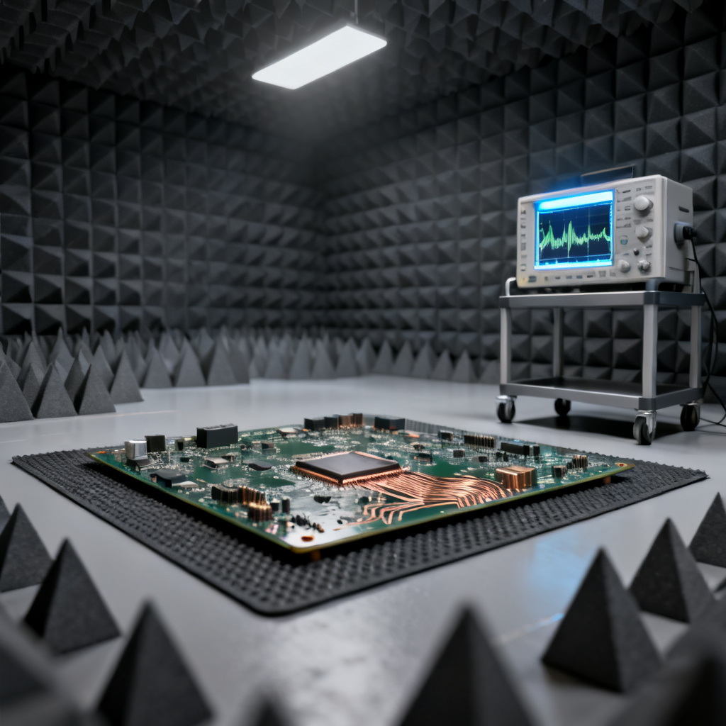
A semi-anechoic chamber (SAC) is a shielded room lined with RF-absorbing material on walls and ceiling, with a reflective conductive floor. This design mimics an open-area test site (OATS) while eliminating external interference and providing consistent, repeatable results.
Controlled Environment for EMI EMC High Speed PCB Testing
Unlike open-air testing, a SAC blocks external radio signals (e.g., broadcast, Wi-Fi, cellular) and prevents reflections from nearby structures. This ensures that measured emissions are solely from your device under test (DUT).
Accuracy for High-Speed Signals
High-speed PCBs (e.g., with clock speeds above 100 MHz or fast rise times) can radiate harmonics into the GHz range. A SAC is calibrated for frequencies from 30 MHz to 18 GHz or higher, covering the full range of emissions from digital circuits.
Compliance with Standards
Most regulatory bodies (FCC, CISPR, EN) accept SAC measurements as equivalent to OATS when the chamber is validated per ANSI C63.4 or CISPR 16-1-4. This makes SAC testing a standard step for CE marking and FCC Part 15 certification.
Preparation and Setup for EMI EMC High Speed PCB Measurements
Proper preparation is essential to avoid false readings and ensure your PCB’s performance is accurately captured.
DUT Placement
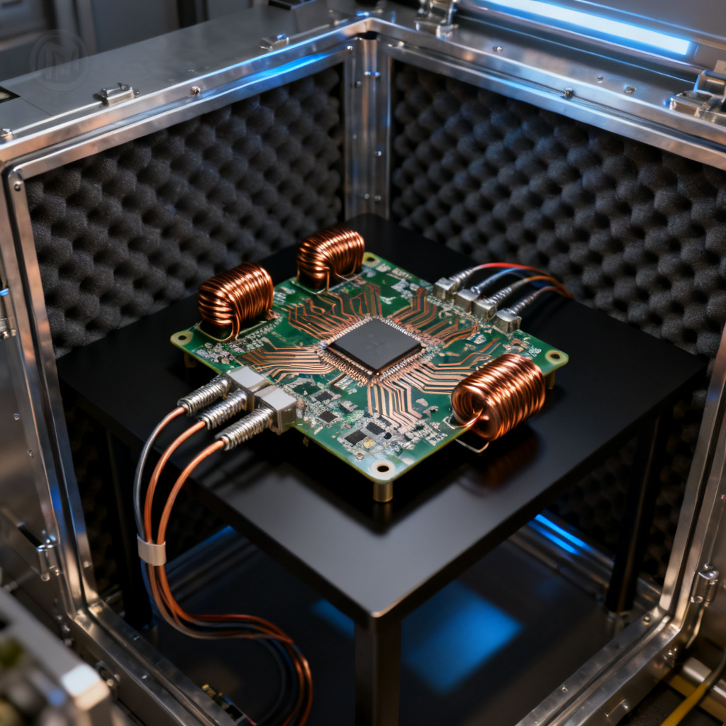
The PCB (or the product containing it) is placed on a non-conductive table at a standard height of 0.8 meters (for tabletop equipment) or on the floor (for floor-standing devices). The orientation should represent the worst-case emission scenario, often rotated 360 degrees during scanning.
Cable Management
High-speed PCBs often connect to external cables (e.g., USB, HDMI, Ethernet). These cables act as antennas. Use ferrite chokes on all cables entering the chamber to isolate the DUT from external noise. Route cables away from the PCB to minimize coupling.
Power Supply
Use a clean, filtered power source inside the chamber. For battery-operated devices, ensure the battery is fully charged and shielded.
Antenna Selection and Placement
For radiated emissions (RE): Use a bilog antenna (30 MHz–1 GHz) and a horn antenna (1–18 GHz). The antenna is placed at a distance of 3 meters or 10 meters from the DUT, depending on the standard. For radiated immunity (RI): Use a log-periodic or horn antenna connected to a power amplifier. The field strength is calibrated using an isotropic field probe.
Calibration
Before testing, perform a site attenuation calibration (NSA test) to confirm the chamber’s performance. The measured attenuation must be within ±4 dB of theoretical values per CISPR 16-1-4.
The Measurement Process for EMI EMC High Speed PCB
Once the DUT is set up, the test proceeds in two main phases: radiated emissions and radiated immunity (if required).
Radiated Emissions (RE) Measurement
Frequency Scan: The receiving antenna sweeps from 30 MHz to 1 GHz (and up to 18 GHz for high-speed designs) using a spectrum analyzer or EMI receiver. The detector is typically set to peak hold, with a resolution bandwidth (RBW) of 120 kHz (for CISPR bands B, C, D) or 1 MHz (for above 1 GHz).
Polarization: The antenna is oriented both vertically and horizontally for each frequency. The DUT is rotated 360 degrees to capture the maximum emission direction.
Identifying Critical Frequencies: At each frequency where emissions exceed the limit minus 6 dB (the “quasi-peak” threshold), the measurement is repeated with quasi-peak detection (for frequencies up to 1 GHz) or average detection (for above 1 GHz). This identifies the worst-case emission.
Data Logging: The system records the amplitude, frequency, polarization, and antenna height (typically 1–4 meters for 3-meter test distance). The final result is the maximum emission level for each frequency.
Radiated Immunity (RI) Measurement (Optional)
Field Generation: The antenna transmits a modulated signal (e.g., 1 kHz AM at 80% depth) at frequencies from 80 MHz to 6 GHz. The field strength is set to the required level (e.g., 3 V/m, 10 V/m for industrial environments).
Monitoring: The DUT’s performance is monitored for degradation. For a PCB, this might include checking for data errors, jitter, or voltage drops. The test is repeated at each frequency step (e.g., 1% increments).
Shielding Effectiveness: For PCBs with enclosures, the chamber can also measure how much external field penetrates the shield.
Expected Results from EMI EMC High Speed PCB Testing
After the test, you’ll receive a report with plots and tables. Here’s how to read it.
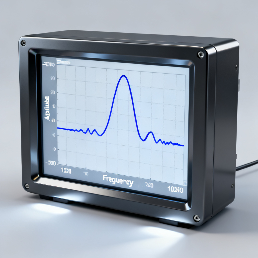
Emissions Plot Interpretation
For high speed PCB EMI and EMC radiated emission testing, the x-axis is frequency (log scale), the y-axis is radiated signal amplitude (dBµV/m). Regulatory limit lines (e.g., FCC Class B: 40 dBµV/m at 30–230 MHz, 47 dBµV/m at 230–1000 MHz) are overlaid on the scan plot. Any spectral peak exceeding the specified emission limit constitutes an EMC failure for the high speed PCB.
Critical Peaks from High-Speed PCBs
Clock Harmonics: Expect strong peaks at the fundamental clock frequency (e.g., 100 MHz) and its harmonics (200 MHz, 300 MHz, etc.). These are often the highest emissions.
Data Bus Noise: Differential pairs (e.g., USB, HDMI) may show lower emissions, but single-ended buses (e.g., DDR memory) can radiate common-mode noise.
Switching Power Supply Ripple: If the PCB includes a DC-DC converter, expect noise at the switching frequency (e.g., 1–5 MHz) and its harmonics.
Margin Analysis
A good design shows at least 6 dB margin below the limit. A margin of 10–20 dB is excellent. If emissions are within 2–3 dB of the limit, consider redesigning the layout or adding shielding.
Immunity Results
If the PCB fails during RI testing (e.g., data corruption at 100 MHz), the report will indicate the vulnerable frequency. This points to specific traces or components that need filtering or rerouting.
Common Challenges in EMI EMC High Speed PCB Measurements
Cable Radiation: External cables often radiate more than the PCB itself. Solution: Use ferrite beads, add common-mode chokes on I/O lines, or integrate filtering into the PCB connector.
Antenna Coupling: At close distances (3 meters), the antenna may couple to the DUT’s near field. Solution: Ensure the DUT is at least 0.5 meters from any absorbing material and use a turntable to find the far-field condition.
Ambient Noise: Even in a SAC, some frequencies (e.g., FM broadcast at 88–108 MHz) may leak through. Solution: Verify the chamber’s shielding effectiveness (SE) is at least 80 dB. If ambient peaks appear, they can be identified by testing with the DUT off.
Temperature Drift: High-speed PCBs generate heat, which can change component behavior. Solution: Run the DUT for 15 minutes before testing to stabilize temperature.
Best Practices for High-Speed PCB Design to Pass EMC Testing
To minimize surprises in the chamber, incorporate these design techniques:
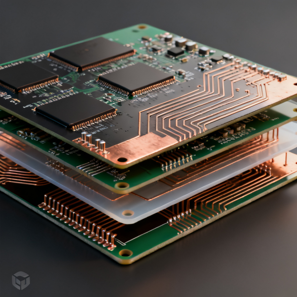
Layer Stack-Up
Use a multi-layer PCB with a solid ground plane. For 4-layer boards, ensure the ground plane is adjacent to the signal layer (e.g., signal-ground-power-signal). This reduces loop area and common-mode radiation.
Decoupling Capacitors
Place 0.1 µF and 10 µF capacitors near each IC power pin to suppress high-frequency noise. Use low-ESL (equivalent series inductance) capacitors for frequencies above 100 MHz.
Trace Routing
Keep high-speed traces (e.g., clock lines) as short as possible. Use 45-degree bends instead of 90-degree corners to reduce reflections. For differential pairs, maintain equal length and impedance.
Shielding
If emissions persist, consider a metal enclosure with good electrical contact (e.g., beryllium copper gaskets). Ensure slots and seams are smaller than 1/20 of the wavelength of the highest frequency.
Pre-Compliance Testing
Use a near-field probe set (e.g., H-field and E-field probes) with a spectrum analyzer to identify hot spots on the PCB before going to the chamber. This reduces the number of iterations.
When to Expect Failures and How to Iterate
Even with careful design, first-time success in a SAC is rare. Here’s a realistic timeline:
First Test: Expect 1–3 failures (e.g., a clock harmonic exceeding the limit by 5 dB). This is normal.
Root Cause Analysis: Use the chamber’s turntable and antenna polarization to locate the emission source. For example, if a peak at 200 MHz is strongest when the antenna is horizontal and the DUT is at 90 degrees, the culprit is likely a horizontal trace on the top layer.
Mitigation: Add a ferrite bead on the trace, increase the ground plane cutout, or reroute the trace to a lower layer. Then retest.
Second Test: After fixes, expect to pass or have marginal failures. Often, a single redesign cycle is sufficient for high-speed PCBs.
Choosing a Test Lab or Conducting In-House Testing
Third-Party Lab: Use an accredited lab (e.g., UL, TÜV, Intertek) for certification. They provide a full report accepted by regulators. Cost: $1,000–$5,000 per day.
In-House SAC: For repeated testing, invest in a pre-compliance chamber (e.g., 3-meter SAC). Ensure it meets NSA requirements. Cost: $50,000–$200,000.
What to Expect from a Lab: They will handle setup, calibration, and reporting. You provide the DUT, power supply, and any necessary cables. The test takes 1–2 days for emissions and immunity.
Comparison: In-House vs. Third-Party EMI EMC High Speed PCB Testing
| Parameter | In-House Testing | Third-Party Lab |
|---|---|---|
| Cost | $50,000–$200,000 initial investment | $1,000–$5,000 per day |
| Time to Results | Immediate after setup | 1–2 days |
| Regulatory Acceptance | Requires validation | Full certification accepted |
| Flexibility | High (test as needed) | Low (scheduled slots) |
| Expertise Required | High (in-house engineer) | Low (provided by lab) |
EMI EMC High Speed PCB Testing Specifications Table
| Parameter | Specification |
|---|---|
| Frequency Range (Emissions) | 30 MHz – 18 GHz |
| Frequency Range (Immunity) | 80 MHz – 6 GHz |
| Test Distance | 3 m or 10 m |
| Antenna Types | Bilog (30 MHz–1 GHz), Horn (1–18 GHz) |
| Resolution Bandwidth | 120 kHz (CISPR), 1 MHz (above 1 GHz) |
| Detector Modes | Peak, Quasi-Peak, Average |
| Field Strength (Immunity) | 3 V/m, 10 V/m |
FAQ: EMI EMC High Speed PCB Measurements in a Semi-Anechoic Chamber
What is the purpose of EMI EMC High Speed PCB measurements in a semi-anechoic chamber?
How should I prepare my high-speed PCB for EMI EMC High Speed PCB testing?
What are common failures during EMI EMC High Speed PCB measurements?
What is the difference between a semi-anechoic chamber and an open-area test site for EMI EMC High Speed PCB testing?
How do I interpret the results from EMI EMC High Speed PCB measurements?
Glossary of EMI EMC High Speed PCB Terms
- EMI (Electromagnetic Interference): Unwanted electromagnetic energy that disrupts the operation of electronic devices.
- EMC (Electromagnetic Compatibility): The ability of a device to function without causing or suffering from EMI.
- Semi-Anechoic Chamber (SAC): A shielded room with RF-absorbing material on walls and ceiling, used for testing emissions and immunity.
- Radiated Emissions (RE): Unintended electromagnetic energy radiated from a device.
- Radiated Immunity (RI): The ability of a device to withstand external electromagnetic fields.
- NSA (Normalized Site Attenuation): A calibration test to validate the performance of a semi-anechoic chamber.
Why Choose Our High-Speed PCB Manufacturing for EMI EMC Compliance
Our high-speed PCB manufacturing services specialize in designs that minimize EMI and maximize EMC performance. We offer controlled impedance stackups, advanced decoupling strategies, and pre-compliance testing support. Unlike generic PCB suppliers, we provide EMI EMC High Speed PCB measurements as part of our design review process, ensuring your product meets regulatory standards from the first prototype.