EMI EMC high speed PCB designs with high-frequency clocks, DDR, Ethernet, USB, HDMI, and PAM4 signaling easily suffer from excessive EMI radiation and EMC compliance failures. Mastering EMI EMC high speed PCB principles is essential for product certification. Uncontrolled return paths, split reference planes, large loop areas, poor stackup, and unfiltered I/O cables become the main antenna sources of electromagnetic noise.
This ultimate pillar guide combines industry-standard principles from Cadence, Academy of EMC, and Sierra Circuits, covering EMI EMC high speed PCB basic definitions, radiation mechanisms, loop area antenna effect, stackup optimization, grounding rules, clock guard routing, filtering & shielding, I/O EMC handling, global EMI standards, pre-compliance testing, troubleshooting workflow, common problems & fixes, and a ready-to-use EMI/EMC design checklist.
Whether you are a hardware engineer, PCB layout designer, electronics buyer, or product developer, you can follow this step-by-step framework to design high-speed PCBs that pass FCC, CISPR, and EN EMC certification on the first try. Proper EMI EMC high speed PCB design starts with understanding the fundamental principles covered in this guide.
Table of Contents
- 1. What Are EMI and EMC in High-Speed PCB Design
- 2. Main Sources of EMI Radiation in High-Speed PCB
- 3. Loop Area: The Fundamental Antenna Effect of PCB EMI
- 4. Core EMI & EMC Suppression Design Methods
- 5. Global EMI Standards and Class B Radiation Limits
- 6. Pre-Compliance Testing Methods for High-Speed PCB
- 7. Step-by-Step EMI Troubleshooting & Fault Location Workflow
- 8. Common EMI Problems, Root Causes and Practical Solutions
- 9. Complete EMI/EMC Design Checklist for High-Speed PCB Layout
- 10. Key Takeaways
- 11. FAQ About High-Speed PCB EMI and EMC Design
- 12. Get Professional PCB EMI/EMC Design Review & Compliance Support
1. What Are EMI and EMC in High-Speed PCB Design
As digital systems move from hundreds of Mbps to multi-Gbps NRZ and PAM4 signaling, high-speed PCBs become the backbone of modern embedded, communication, industrial, and consumer electronics. Signal edge rates become faster, harmonic frequency components become richer, and electromagnetic interference naturally becomes one of the biggest challenges for product certification and stable operation. Understanding EMI EMC high speed PCB principles is essential for every hardware engineer, just as return path integrity forms the foundation of signal integrity discussed in our Return Path Design Guide. Achieving EMI EMC high speed PCB compliance requires intentional design from the very beginning.
Definition of EMI
EMI (Electromagnetic Interference) refers to unwanted electromagnetic energy radiated or conducted by PCB traces, components, power planes, and external cables. This noise can interfere with nearby sensitive analog circuits, low-signal sensors, wireless modules, and other electronic equipment in the working environment. Controlling high-speed PCB EMI design is critical for product reliability and EMI EMC high speed PCB certification.
Definition of EMC
EMC (Electromagnetic Compatibility) means an electronic device can operate normally in a complex electromagnetic environment without emitting excessive interference and without being easily disturbed by external electromagnetic noise. Achieving PCB EMC compliance guidelines requires intentional design from the start, which is the core goal of any EMI EMC high speed PCB project.
Core Contradiction in High-Speed PCB
High-frequency and high-speed signals inherently generate rich harmonics. Fast rise/fall edges, periodic clock signals, and long I/O cables act like natural antennas. This makes high-speed PCBs far more likely to fail EMI emission tests than low-speed designs. Good EMI EMC high speed PCB design is not an afterthought — it must be planned from stackup, schematic selection, component placement, and routing layout.
2. Main Sources of EMI Radiation in High-Speed PCB
All high-speed PCB EMI design issues can be categorized into three root sources: common-mode radiation, differential-mode radiation, and unique radiation characteristics of different high-speed signal types. Understanding these sources is fundamental to EMI EMC high speed PCB analysis.
2.1 Common-Mode Radiation
Common-mode radiation is the dominant cause of far-field EMI failure in most commercial products — especially when signals cross split reference planes. In EMI EMC high speed PCB design, this is one of the most critical issues to address. As detailed in our Return Path Design Guide, crossing a plane split forces return current to detour around the gap instead of flowing directly underneath the signal trace. This detour creates a large current loop that acts as an efficient radiating antenna, producing strong common-mode noise that easily exceeds FCC and CISPR limits.
Main triggers: Signal traces crossing reference plane splits, long ungrounded ground traces, unshielded external I/O cables
Frequency impact: Mainly dominates 30 MHz – 1 GHz radiation and easily exceeds Class B limits
2.2 Differential-Mode Radiation
Differential-mode radiation mainly affects near-field coupling inside the PCB board. Formed by the closed loop of signal trace and its return current path, larger loop area creates stronger near-field radiation and crosstalk. Poor routing, discontinuous return paths, and randomly placed decoupling capacitors will expand loop size and worsen internal interference. Managing loop area is a key EMI EMC high speed PCB technique.
2.3 Radiation Characteristics of Typical High-Speed Signals
Different signal types have completely different spectral features and EMI behaviors. Understanding these characteristics — such as how clock jitter generates harmonic spikes — is essential for targeted suppression, a topic covered in our Eye Diagram and Jitter Analysis Guide. Successful EMI EMC high speed PCB design requires analyzing each signal type’s unique radiation profile.
| Signal Type | Radiation & Spectrum Characteristics |
|---|---|
| Clock / Periodic Signals | Discrete high-amplitude harmonic spikes; obvious single peaks in EMI spectrum |
| PRBS High-Speed Data | Continuous wideband spectrum; smooth broadband noise floor elevation |
| PAM4 Signals | More abundant frequency components than NRZ; wider radiation bandwidth and denser harmonic distribution |
Mixed integration of clock, data, and communication signals will superimpose noise and greatly increase PCB EMC compliance design difficulty, making EMI EMC high speed PCB expertise essential.
3. Loop Area: The Fundamental Antenna Effect of PCB EMI
The most essential rule of EMI EMC high speed PCB design: the signal return loop is an antenna. Every high-speed PCB EMI design decision should consider loop area minimization.
Radiated electric field strength follows a core physical formula:
E ∝ I × A × f²
Where: E = Radiated electric field strength, I = Loop current magnitude, A = Enclosed loop area, f = Signal working frequency.
The formula clearly explains why high-speed circuits are much harder for PCB EMC compliance guidelines: radiation increases with the square of frequency. Higher frequency means exponentially stronger radiation. This is why EMI EMC high speed PCB design becomes increasingly critical as data rates rise.
How to Minimize Loop Area at the Source
- Use complete solid ground reference planes to keep return current directly underneath signal traces
- Maintain ground plane continuity; avoid unnecessary slots and splits
- Place high-speed signal layers tightly adjacent to ground layers for strong trace-ground coupling
- Avoid long detoured return paths caused by plane splitting
By shrinking the radiation loop, you suppress EMI from the physical root instead of fixing it after board production. This is the most cost-effective high-speed PCB EMI design technique and the foundation of successful EMI EMC high speed PCB design.
4. Core EMI & EMC Suppression Design Methods
This chapter integrates stackup, reference plane design, clock guard routing, filtering, shielding, and I/O region processing — the complete system used by Cadence, Sierra Circuits and mainstream industrial design standards for EMI EMC high speed PCB compliance.
4.1 PCB Stackup Design Rules
PCB stackup determines electromagnetic field distribution and noise suppression capability from the beginning for EMI EMC high speed PCB:
- Signal-GND tight coupling: Restrain electromagnetic field diffusion and reduce stray radiation
- High-speed signals routed as inner stripline: Stripline on inner layers can reduce radiation by about 20 dB compared with surface microstrip lines — a key EMI EMC high speed PCB advantage
- Thin dielectric between Power and GND planes: This forms distributed planar capacitance — a key principle also covered in our Power Integrity Guide for PDN optimization and broadband EMI suppression
4.2 Keep Reference Plane Integrity
High-speed traces must never cross split or slotted ground/power planes. Crossing splits cuts the shortest return path, forces current to detour, creates huge loop area, and triggers severe common-mode and differential-mode radiation. This is a fundamental rule of EMI EMC high speed PCB layout. For mixed-signal boards with DDR, RF, analog, and digital circuits, perform functional zoning but use ground bridges to maintain overall ground continuity. Avoid isolated ground islands that become parasitic radiation antennas.
4.3 Clock & High-Frequency Signal Guard Routing
Clocks are the biggest harmonic radiation source and need dedicated protection in high-speed PCB EMI design:
- Add guard ground traces on both sides of clock lines
- Ground via spacing along guard route ≤ 100 mil or λ/10 of the working wavelength
- Guard trace width ≥ 10 mil for sufficient grounding and shielding
- Avoid routing other traces underneath clock lines
4.4 Filtering and Shielding Technology
- Common-mode chokes: Applied on USB, Ethernet, HDMI, and high-speed differential interfaces to filter board-level common-mode noise and stop cable radiation — essential for EMI EMC high speed PCB compliance
- EMI filters: Placed at power entry and sensitive analog power ports to suppress conducted interference and switching ripple
- Metal shielding covers: Enclose clock oscillators, RF modules, and high-noise circuits to isolate internal radiation and external interference
4.5 I/O Region EMC Design
The I/O interface area is the main channel for noise to radiate out through external cables in PCB EMC compliance guidelines and EMI EMC high speed PCB design:
- Place filter circuits and ferrite components close to interface connectors
- Adopt reasonable ground splitting for digital and analog domains; use bridge capacitors or ferrite beads for potential balance and noise isolation
- Use shielded connectors with 360° metal shell bonding to maintain shielding integrity and eliminate cable antenna effects
4.6 Advanced Hidden EMI Risks
- Remove floating unused traces and isolated copper islands; floating conductors act as hidden antennas that undermine EMI EMC high speed PCB performance
- Add edge copper grounding on PCB borders to reduce edge radiation and improve shielding
- Place decoupling capacitors as close to IC pins as possible; dense ground vias reduce impedance and noise coupling
5. Global EMI Standards and Class B Radiation Limits
All commercial high-speed PCB products must comply with international EMC emission standards before mass production. Understanding EMI EMC high speed PCB requirements means knowing which standards apply to your product and target market.
| Region | Official EMC Standard |
|---|---|
| International | CISPR 22 / CISPR 32 |
| United States | FCC Part 15 |
| European Union | EN 55032 (Information Technology Equipment) |
Class B 3m Chamber Radiation Limits (Civil Commercial Products)
| Frequency Band | Quasi-Peak (dBμV/m) | Average (dBμV/m) |
|---|---|---|
| 30–230 MHz | 40 | — |
| 230–1000 MHz | 47 | — |
| 1–6 GHz Radiated Emission | 50–54 | 40–44 |
All layout and stackup design must reserve sufficient margin below these limits to pass formal certification. Meeting these standards is the ultimate goal of any EMI EMC high speed PCB project.
6. Pre-Compliance Testing Methods for High-Speed PCB
Avoid costly formal certification failures by conducting pre-testing at the prototype stage for high-speed PCB EMI design and EMI EMC high speed PCB validation:
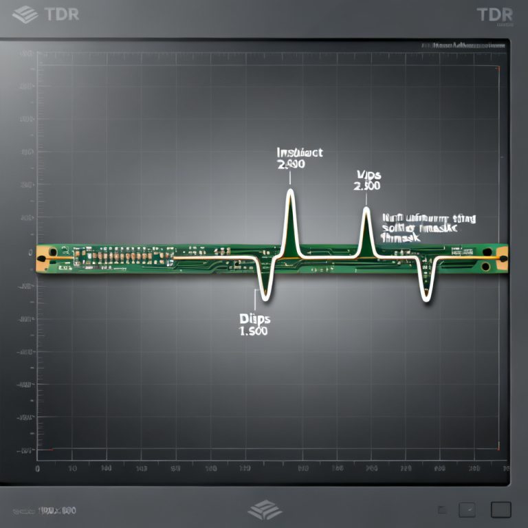
- Near-field probe scanning: Fast locate EMI hotspots and high-radiation areas on PCB
- Spectrum analyzer manual scanning: Capture full-band spectrum and pinpoint exact over-limit frequency points
- Semi-anechoic chamber pre-test: Simulate official 3m test environment, verify margin, and reserve space for optimization and revision
Early pre-testing can find hidden design defects and reduce board revision times, accelerating your EMI EMC high speed PCB certification process.
7. Step-by-Step EMI Troubleshooting & Fault Location Workflow
Follow this standardized process to debug EMI EMC high speed PCB issues efficiently without blind modification:
- Capture full-band spectrum with a spectrum analyzer and confirm which frequency points exceed limits
- Use near-field probe scanning to locate specific PCB physical areas with abnormal radiation
- Analyze suspected noise sources: clock harmonics, switching power supply ripple, high-speed data bus coupling
- Perform module isolation test: idle/load switching to lock the exact interference source
- Apply countermeasures: add decoupling capacitors, optimize grounding, install filters, add shielding, adjust routing
- Re-test and verify improvement until meeting Class B limits
This systematic approach is essential for successful EMI EMC high speed PCB debugging and certification.
8. Common EMI Problems, Root Causes and Practical Solutions
| EMI Phenomenon | Root Cause | Professional Solution |
|---|---|---|
| Broadband noise floor overall elevated | Poor PDN impedance, insufficient decoupling | Add high-frequency low-ESR decoupling capacitors; optimize stackup |
| Single sharp spectral spike | Periodic clock oscillator radiation | Apply π-type filter, reduce driver strength, clock guard routing |
| 100–300 MHz wideband noise envelope | Uncontrolled high-speed data bus radiation | Reduce signal edge rate, inner layer routing, interlayer shielding |
| Noise leaking from I/O ports | Common-mode noise coupled to cables | Install common-mode chokes, add magnetic rings, shielded cables |
9. Complete EMI/EMC Design Checklist for High-Speed PCB Layout
Use this checklist at schematic and layout stage to avoid inherent PCB EMC compliance defects and ensure EMI EMC high speed PCB success:
- Route all critical high-speed signals on inner layers as stripline instead of surface microstrip
- Ensure every high-speed signal has continuous, unbroken solid reference planes
- Apply guard routing and dense grounding vias for all clock and high-frequency oscillator traces
- Strictly prohibit high-speed traces crossing ground or power plane splits
- Place EMI filters, ferrite beads, and decoupling capacitors close to I/O interfaces and power inlets
- Reserve reliable grounding pads for metal enclosures to maintain 360° shielding continuity
- Equip all high-speed external interfaces with common-mode chokes and necessary filter components
- Remove floating copper, unused stubs, and isolated island copper to eliminate hidden antenna sources
10. Key Takeaways for EMI EMC High Speed PCB Design
- Loop area and discontinuous return paths are the primary root of EMI EMC high speed PCB radiation. Minimizing loop size is the most cost-effective design rule.
- Inner-layer stripline routing reduces radiation by around 20 dB compared with surface traces — prioritize this for high-speed critical signals in high-speed PCB EMI design and EMI EMC high speed PCB projects.
- Complete reference planes, clock guard routing, filtering, and shielding form the four core pillars of PCB EMC compliance guidelines.
- Follow global standards (FCC Part 15, CISPR 32, EN 55032) and reserve sufficient test margin in early design.
- Conduct pre-compliance testing and follow standardized troubleshooting flow to shorten debug cycle and reduce board revisions.
- Use the EMI/EMC design checklist throughout layout to achieve one-pass EMC certification. Successful EMI EMC high speed PCB design requires attention to every detail covered in this guide.
11. FAQ About High-Speed PCB EMI and EMC Design
Q1: Why do high-speed PCBs easily fail EMI tests?
Fast signal edge rates generate rich high-order harmonics; large return loop areas, split reference planes, and unshielded I/O cables act as antennas to radiate noise outward. Proper EMI EMC high speed PCB design addresses these root causes — starting with the return path integrity principles covered in our Return Path Design Guide.
Q2: Is inner layer routing always better for EMC?
Yes. Inner stripline is tightly coupled with upper/lower ground planes, suppressing field leakage and reducing radiation by about 20 dB versus surface microstrip lines. This is a key high-speed PCB EMI design technique and a cornerstone of EMI EMC high speed PCB best practice.
Q3: What is the biggest EMI risk of crossing reference plane splits?
Crossing splits cuts the natural shortest return path, forces return current to detour, creates a huge radiation loop, and causes severe common-mode far-field radiation. Following PCB EMC compliance guidelines means never crossing splits — a rule explained in depth in our Return Path Guide and critical for EMI EMC high speed PCB success.
Q4: Do I need a common-mode choke for all high-speed interfaces?
For USB, Ethernet, HDMI, and differential communication interfaces, adding a common-mode choke is the most effective way to suppress cable common-mode radiation and pass EMC tests. This is a standard EMI EMC high speed PCB practice.
Q5: When should we start EMC design for PCB?
EMC must be considered from stackup planning, schematic component selection, and component placement — not fixed after layout is finished. EMI EMC high speed PCB design starts at the very beginning, alongside your power integrity strategy discussed in our Power Integrity Guide.
Get Professional PCB EMI/EMC Design Review & Compliance Support
If you are developing high-speed digital boards, industrial control PCBs, communication interface boards, or embedded hardware products and facing these troubles: unsure about stackup design for PCB EMC compliance, prototype keeps failing FCC/EN/CISPR EMI tests, no clear debugging direction, or need standard-compliant layout review — our professional engineering team can help with your EMI EMC high speed PCB project.
We offer: Free professional EMI EMC high speed PCB design review • Custom EMI noise analysis • Stackup optimization • Routing rule guidance • Compliance certification consultation
All design files strictly confidential. Response within one business day.
About HighSpeedPCBs.com
We are a specialized PCB design and manufacturing service provider serving industrial, automotive, medical, and communications OEMs worldwide. Our expertise in EMI EMC high speed PCB design ensures your products pass certification and perform reliably in the field. Return to the Signal Integrity Guide for comprehensive coverage of impedance control, return path design, differential pairs, crosstalk, eye diagram analysis, reflection termination, power integrity, and EMI EMC high speed PCB compliance.
© 2026 HighSpeedPCBs.com — Professional High-Speed PCB Solutions