In high-speed PCB design, impedance control PCB coupon design is the critical quality gate that layout engineers use to verify signal integrity. This pillar page consolidates expert knowledge from leading industry sources to provide you with a definitive guide on designing, placing, and interpreting these coupons. Whether you are a seasoned layout engineer or new to high-speed design, mastering coupon design is essential for ensuring first-pass success.
What Is an Impedance Control PCB Coupon? Definition and Purpose
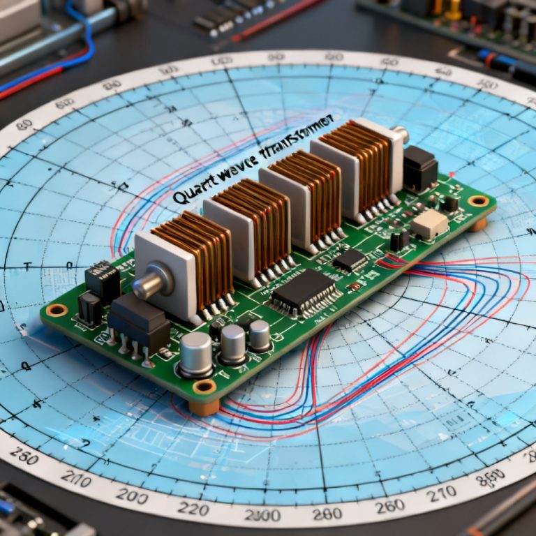
An impedance control PCB coupon (often called a “test coupon” or “impedance test strip”) is a small, sacrificial section of the PCB panel that contains traces designed to replicate the impedance characteristics of the actual circuit board. These coupons are typically located on the breakaway tabs (mouse bites) or the border of the panel and are tested after fabrication to confirm that the PCB manufacturer’s process yields the correct impedance values.
Key Characteristics of an Impedance Control PCB Coupon
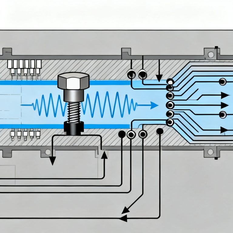
Key characteristics of an impedance control PCB coupon include geometry replication of the same stack-up, dielectric thickness, copper weight, and trace width as the corresponding signals on the main board. Coupons include exposed pads or via structures that allow for Time Domain Reflectometry (TDR) probing. They are sacrificial in nature and are often removed from the panel before shipping, though some manufacturers leave them attached for customer verification.
Why Impedance Control PCB Coupons Matter
Impedance control PCB coupons matter because they validate the manufacturer’s etching, lamination, and plating processes are within tolerance. They confirm that your stack-up assumptions (e.g., Dk values, prepreg thickness) are accurate. Catching impedance issues at the coupon level prevents costly re-spins of the entire board.
Common Types of Impedance Control PCB Coupons
Common coupon types include single-ended microstrip for 50-ohm or custom single-ended traces on outer layers, differential stripline for 100-ohm or 90-ohm differential pairs on inner layers, and edge-coupled vs. broadside-coupled depending on the stack-up and routing topology.
Design Guidelines for Impedance Control PCB Coupons
While the concept is straightforward, poor coupon design can lead to misleading test results. The coupon must be a faithful proxy of the production board.
Trace Length and Termination for Impedance Control PCB Coupons
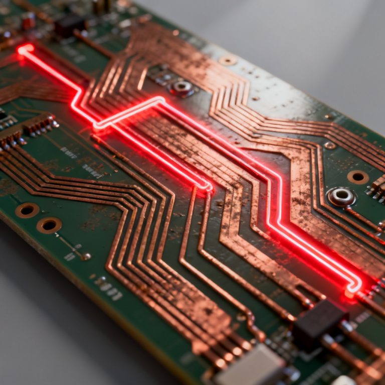
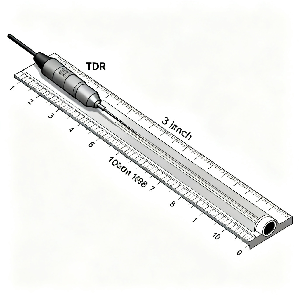
Coupon traces should be at least 3 inches (75 mm) long for accurate TDR measurement. Shorter traces may not allow the TDR to settle, leading to erroneous impedance readings. The far end of the trace must be left open (not terminated) for TDR reflection testing. Do not add a resistor or short the trace.
Layer and Stack-Up Alignment for Impedance Control PCB Coupons
Mirror the stack-up: if your board uses a 0.008-inch prepreg for a specific layer, the coupon must use the same material and thickness. Use the same copper thickness (e.g., 1 oz, 0.5 oz) as the production board. Heavy copper layers will change the impedance profile. Ensure the coupon uses the same laminate and prepreg grades; do not substitute different Dk materials.
Probe Pads and Access for Impedance Control PCB Coupons
Use 50-mil (1.27 mm) diameter pads for standard TDR probes. Smaller pads may cause probe slippage; larger pads can create parasitic capacitance. Place ground vias within 0.1 inches of the signal pad to provide a low-inductance return path for the TDR probe. Maintain a 0.1-inch (2.54 mm) pitch between signal and ground pads for compatibility with standard probe heads.
Avoiding Common Design Mistakes in Impedance Control PCB Coupons
Do not route coupon traces near panel edges: panel edge effects (e.g., glass weave distortion) can skew results. Keep coupon traces at least 0.25 inches from the panel border. Avoid 90-degree bends; use 45-degree or curved corners to minimize reflections within the coupon itself. Include multiple coupons if your board has multiple impedance targets (e.g., 50-ohm single-ended, 100-ohm differential); do not combine them on a single trace.
Advanced Coupon Placement and Panelization Strategies for Impedance Control PCB Coupons
Coupon placement directly impacts test accuracy and panel yield.
Optimal Coupon Location for Impedance Control PCB Coupons
Place coupons on the breakaway tabs adjacent to the board, not on the far edge of the panel. This ensures that the coupon experiences the same plating and etching conditions as the actual circuit. Avoid high-stress areas such as near tooling holes, V-scoring lines, or areas with heavy copper pour. If the panel is large (e.g., >18×24 inches), place coupons at the top, bottom, and center of the panel to capture process variation across the panel.
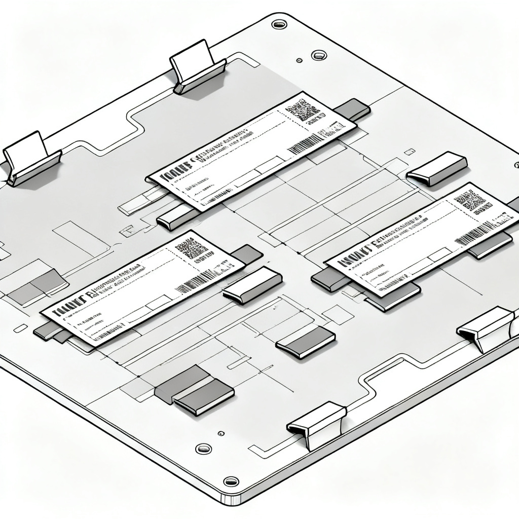
Coupon Size and Number of Traces for Impedance Control PCB Coupons
Standard coupon dimensions are typically 0.5 x 1.5 inches (12.7 x 38.1 mm) per coupon, but this can vary based on the number of test traces. Include 3 to 5 traces per coupon—one for each impedance target plus a spare. For example, a coupon for a 10-layer board might include: 50-ohm microstrip, 100-ohm differential stripline, and 90-ohm differential microstrip. Maintain at least 0.05 inches (1.27 mm) between traces to avoid crosstalk during TDR measurement.
Differential Pair Design in Impedance Control PCB Coupons
Both traces in a differential pair must have identical lengths, widths, and spacing. Any asymmetry will cause common-mode noise and skew. Ensure that the differential pair has a continuous ground plane on the adjacent layer; do not allow splits or voids in the reference plane under the coupon traces. If the coupon includes vias (for stripline testing), use two vias per pair—one for each signal—and keep the via stubs as short as possible. Avoid through-hole vias for high-frequency coupons.
Panelization and Coupon Removal for Impedance Control PCB Coupons
Use mouse bites or V-grooves that allow easy removal of the coupon after testing. Avoid scoring that could damage the coupon traces. Some manufacturers offer to leave coupons attached for customer-side TDR verification; specify this in your fabrication notes if needed. Include a coupon map in your fabrication drawing showing the exact location and impedance target for each coupon.
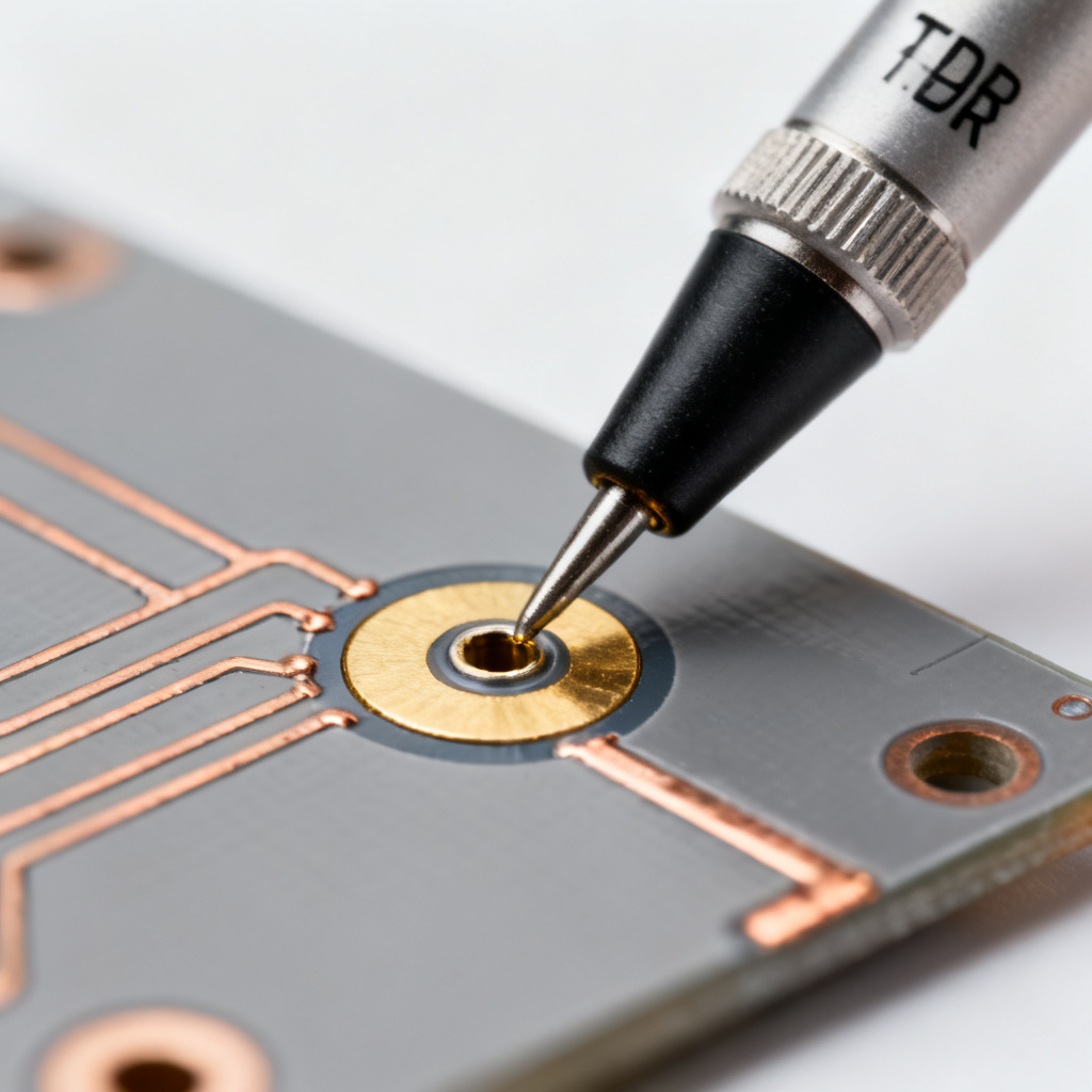
Testing and Interpreting Impedance Control PCB Coupon Results
Testing and interpreting impedance control PCB coupon results requires proper TDR measurement setup and understanding of acceptable tolerances.
TDR Measurement Setup for Impedance Control PCB Coupons
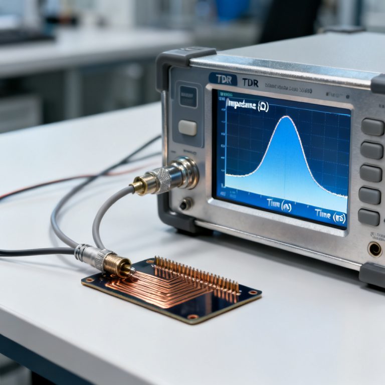
Use a TDR with a rise time of 35 ps or faster for accurate impedance measurement at frequencies up to 10 GHz. Calibrate the TDR to the probe tip using a known open, short, and 50-ohm load. Probe the coupon at the signal pad, ensuring good contact with the ground via.
Acceptable Tolerance for Impedance Control PCB Coupons
Industry standard is ±10% for most designs (e.g., 50-ohm target: 45-55 ohms). High-speed designs (e.g., PCIe Gen 5, USB 3.2) require ±5% or tighter. If the coupon fails, do not immediately assume a manufacturing error; check your stack-up calculations, Dk assumptions, and coupon design first.
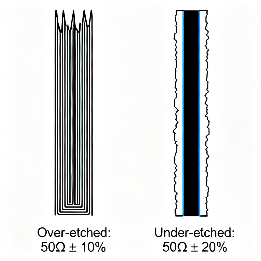
Common Failure Modes and Root Causes in Impedance Control PCB Coupons
Impedance too high is often due to over-etching (trace width too narrow) or dielectric thickness greater than specified. Impedance too low is caused by under-etching (trace width too wide), thinner dielectric, or higher Dk than expected. Non-uniform impedance along the trace suggests process variation (e.g., uneven plating) or glass weave effect; consider using a tighter weave glass or spread glass.
When to Redesign vs. Accept Based on Impedance Control PCB Coupon Results
If the coupon fails but the production board passes functional tests (e.g., eye diagram), you may accept the deviation—but document it. If the coupon fails and the production board shows signal integrity issues, request a stack-up re-optimization or etch compensation from the manufacturer.
Best Practices Summary for Impedance Control PCB Coupon Design
Based on the collective wisdom from all three sources, here is a checklist for layout engineers:
- Include a dedicated coupon for each unique impedance target on your board.
- Design coupons with minimum 3-inch trace length and open termination for TDR.
- Place coupons on breakaway tabs near the production board, not on the panel edge.
- Use 50-mil probe pads with adjacent ground vias for reliable TDR access.
- Specify Dk values and stack-up tolerances in your fabrication notes—do not assume the manufacturer will use your assumed values.
- Request a coupon map in your fabrication drawing to avoid confusion.
- Test coupons from multiple panel locations if the board is large or high-volume.
- Maintain a ±5% impedance tolerance for high-speed differential pairs (e.g., 100-ohm ±5 ohms).
- Document coupon results in your design history for future reference.
Impedance Control PCB Coupon Design: Comparison of Approaches
When comparing impedance control PCB coupon design approaches, the industry-leading method involves placing coupons on breakaway tabs near the board to replicate manufacturing conditions, while a less effective approach places coupons on the panel edge where process variation is higher. Our recommended approach (using multiple panel locations and dedicated coupons per target) provides superior accuracy and first-pass yield compared to single-coupon designs.
Key Terminology in Impedance Control PCB Coupon Design
Understanding key terminology is essential for layout engineers: Time Domain Reflectometry (TDR) is the primary measurement method for impedance verification. Dielectric constant (Dk) refers to the material’s ability to store electrical energy and directly affects impedance. Etch compensation adjusts trace widths to account for copper removal during fabrication. Glass weave effect describes impedance variation caused by the non-uniform distribution of glass fibers in the laminate.
Frequently Asked Questions About Impedance Control PCB Coupon Design
What is the primary purpose of an impedance control PCB coupon?
The primary purpose of an impedance control PCB coupon is to verify that the fabricated PCB meets the target impedance specifications, ensuring signal integrity in high-speed designs.
How long should an impedance control PCB coupon trace be?
An impedance control PCB coupon trace should be at least 3 inches (75 mm) long for accurate TDR measurement.
What is the acceptable tolerance for impedance control PCB coupons?
Industry standard tolerance for impedance control PCB coupons is ±10% for most designs, but high-speed designs require ±5% or tighter.
Where should I place impedance control PCB coupons on the panel?
Impedance control PCB coupons should be placed on breakaway tabs adjacent to the production board, not on the panel edge, to ensure accurate replication of manufacturing conditions.
What causes impedance control PCB coupon failure?
Common causes of impedance control PCB coupon failure include over-etching, under-etching, incorrect dielectric thickness, or process variation across the panel.
Impedance Control PCB Coupon Specifications Table
| Parameter | Impedance Control PCB Coupon Specification | Recommended Value |
|---|---|---|
| Trace Length | Impedance control PCB coupon minimum length | 3 inches (75 mm) |
| Probe Pad Diameter | Impedance control PCB coupon pad size | 50 mil (1.27 mm) |
| Ground Via Distance | Impedance control PCB coupon via proximity | 0.1 inches (2.54 mm) |
| Trace Spacing | Impedance control PCB coupon trace-to-trace | 0.05 inches (1.27 mm) |
| Impedance Tolerance | Impedance control PCB coupon tolerance | ±10% (standard), ±5% (high-speed) |
| Coupon Dimensions | Impedance control PCB coupon size | 0.5 x 1.5 inches (12.7 x 38.1 mm) |
Impedance control PCB coupons are not an afterthought—they are a critical quality gate between design and manufacturing. By following the design guidelines, placement strategies, and testing protocols outlined in this pillar page, you can ensure that your high-speed PCBs meet impedance specifications consistently. Remember: a well-designed coupon saves time, money, and frustration. Incorporate coupon design into your layout process from day one, and you will achieve higher first-pass yield and reliable signal integrity.
“`