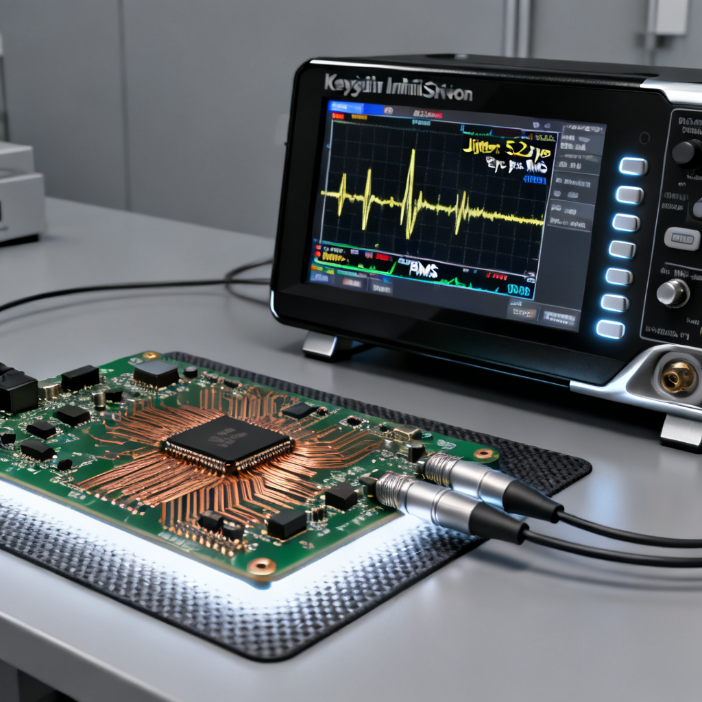
Master jitter analysis for high-speed PCB designs using Keysight InfiniiVision oscilloscopes. This guide covers measurement techniques, jitter decomposition, and practical troubleshooting steps to ensure signal integrity.
Understanding Jitter Fundamentals for High Speed PCB
In high-speed PCB design, even picoseconds of timing uncertainty—known as jitter—can corrupt data and cause bit errors. Jitter analysis measures and decomposes these timing deviations. The industry standard classifies jitter into two main categories.
Random Jitter (RJ)
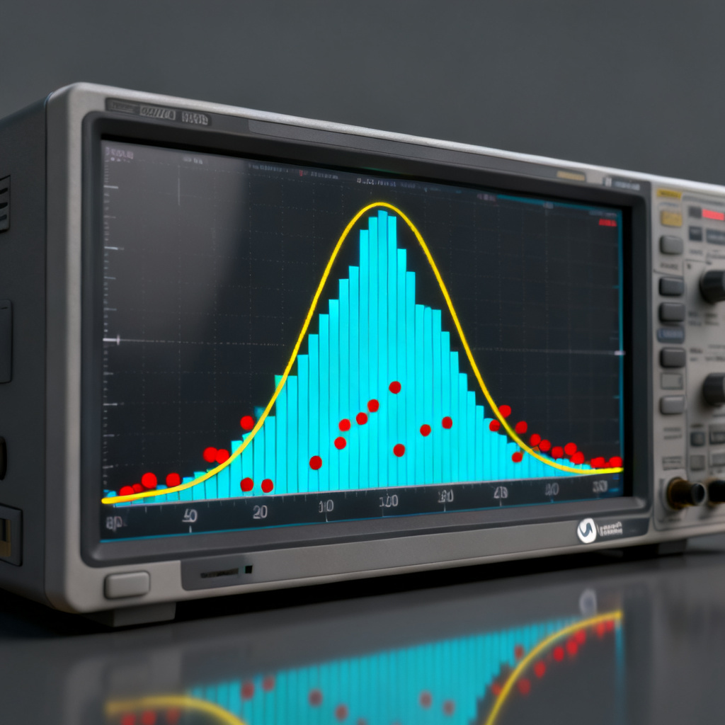
Random jitter (RJ) is caused by thermal noise, shot noise, and semiconductor flicker noise. It follows a Gaussian distribution and is unbounded. Jitter analysis typically reports RJ as an RMS value.
Deterministic Jitter (DJ)
Deterministic jitter (DJ) is bounded and predictable, arising from data-dependent or periodic sources. Subtypes include periodic jitter (PJ) from power supplies, data-dependent jitter (DDJ) from impedance mismatches, duty-cycle distortion (DCD), and bounded uncorrelated jitter (BUJ) from crosstalk.
Key Jitter Metrics for High Speed PCB
| Metric | Description | Relevance in High Speed PCB |
|---|---|---|
| TIE (Time Interval Error) | Deviation of a clock edge from its ideal position | Fundamental measurement for jitter analysis |
| Peak-to-Peak Jitter | Total spread of edge timing including RJ and DJ | Grows with measurement time due to RJ |
| RMS Jitter | Standard deviation of TIE distribution | Used to characterize random jitter |
| Total Jitter (TJ) | Extrapolated at BER 10^-12 | Critical for high-speed serial link compliance |
Setting Up Keysight InfiniiVision for Jitter Analysis in High Speed PCB
Proper setup is essential for accurate jitter analysis. Follow these hardware and software configuration steps.
Hardware Configuration for Jitter Analysis
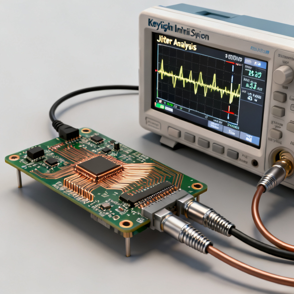
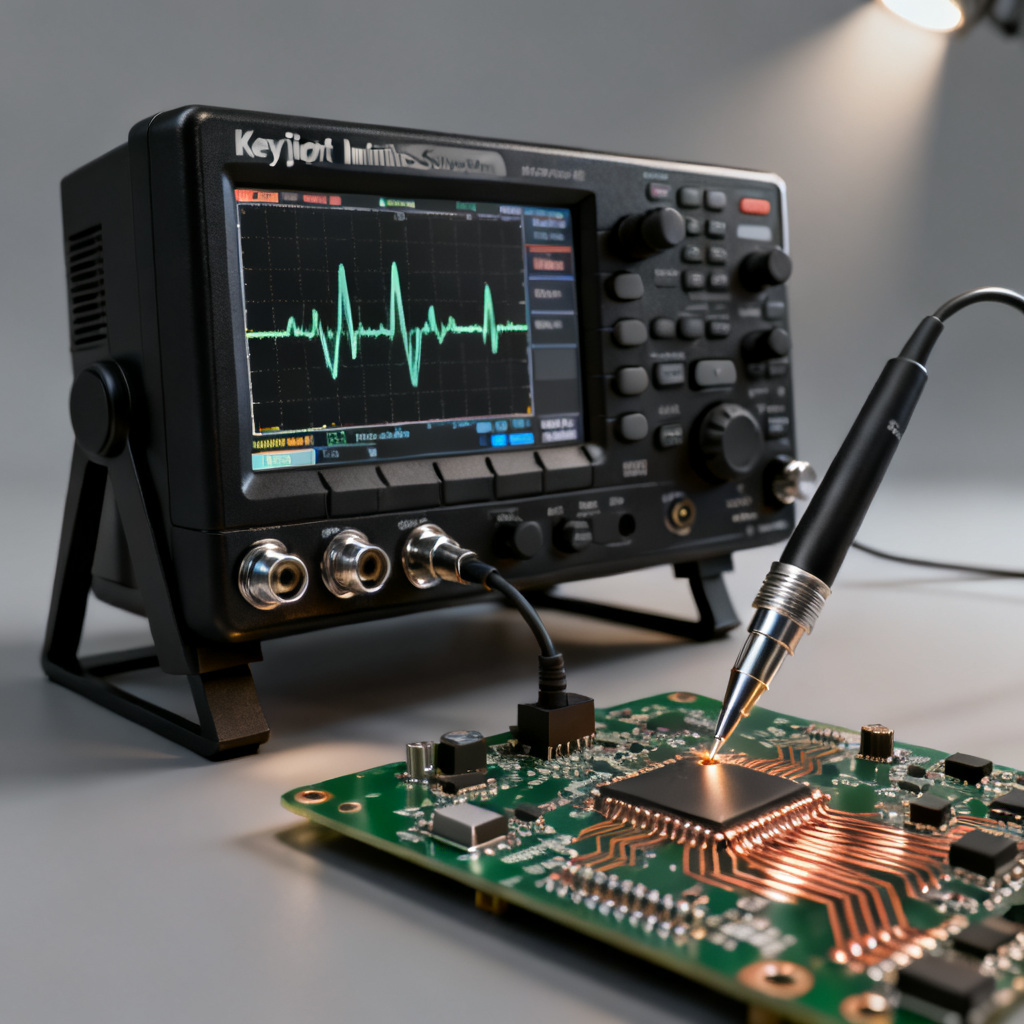
Use a high-bandwidth, low-noise active probe (e.g., Keysight N2790A) to avoid adding jitter. For differential signals like LVDS or PCIe, use a differential probe. Keep the ground lead shorter than 1 cm to minimize ground bounce.
Acquisition Settings for High Speed PCB Jitter Analysis
Set the sampling rate to maximum (5 GSa/s on 4000 X, 10 GSa/s on 6000 X). Use deep memory (4 Mpts) to capture over 100,000 edges for statistically significant measurements. Adjust the timebase to display 10-20 clock cycles.
Enabling Jitter Analysis on Keysight InfiniiVision
Press Analyze > Jitter Analysis (or Jitter on MXR models). Select the source channel and choose TIE (Time Interval Error) as the measurement type. Set the threshold level to 50% for CMOS/LVDS signals.
Performing Jitter Analysis Measurement on High Speed PCB
With the oscilloscope configured, execute the jitter analysis measurement.
Capture the Waveform for Jitter Analysis
Ensure the waveform is stable. Use Single acquisition to capture a clean waveform. Avoid infinite persistence as it masks transient jitter events.
Run Jitter Analysis on Keysight InfiniiVision
After enabling jitter analysis, the oscilloscope automatically computes the jitter histogram, jitter vs. time plot, and bathtub curve. On 6000 X and MXR models, view the jitter spectrum (FFT of TIE) to identify periodic jitter frequencies.
Interpret Jitter Analysis Results
A Gaussian histogram indicates dominant random jitter. Bimodal or skewed distributions suggest deterministic jitter. The jitter vs. time plot reveals periodic patterns from power supplies or crosstalk. The bathtub curve shows the eye opening at BER 10^-12.
Decomposing Jitter for High Speed PCB Troubleshooting
The InfiniiVision’s jitter decomposition feature separates RJ and DJ using a dual-Dirac model. This helps identify root causes.
Separate RJ and DJ in Jitter Analysis
Use the Jitter Decomposition feature (available on MXR and 6000 X with Option DJA). RJ is reported as 1-sigma RMS, and DJ is reported as peak-to-peak.
Identify DJ Subtypes in High Speed PCB
Periodic jitter (PJ) appears as peaks in the jitter spectrum. Data-dependent jitter (DDJ) is visible in the eye diagram as asymmetrical closing. Duty-cycle distortion (DCD) shows as a deviation from 50% duty cycle.
Advanced Jitter Analysis Techniques
Use the trend analysis plot to correlate jitter with external events. On MXR models, gate the histogram to isolate edge-dependent jitter. This is critical for high-speed PCB validation.
Practical Troubleshooting for High Speed PCB Jitter
Based on jitter decomposition, apply these fixes to common high-speed PCB issues.
High Periodic Jitter (PJ) in High Speed PCB
Root cause: power supply ripple or EMI. Fix: add decoupling capacitors (0.1 µF + 1 µF) near IC power pins. Use ferrite beads on power lines.
High Data-Dependent Jitter (DDJ) in High Speed PCB
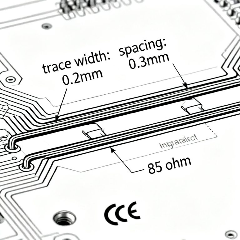
Root cause: impedance mismatch or stub reflections. Fix: simulate trace impedance (target 50Ω ±10%). Add series termination resistors near the driver.
Duty-Cycle Distortion (DCD) in High Speed PCB
Root cause: asymmetric driver or threshold offset. Fix: replace the driver if duty cycle exceeds 55% or falls below 45%.
Excessive Random Jitter (RJ) in High Speed PCB
Root cause: thermal noise or weak driver. Fix: increase signal swing. Use a lower-noise LDO for the clock PLL.
Advanced Keysight InfiniiVision Features for Jitter Analysis
Leverage hardware-accelerated jitter measurements for real-time updates. MegaZoom IV technology enables responsive zoom and pan. Mask testing combines jitter analysis with eye-diagram compliance. Segmented memory captures intermittent jitter events.
Best Practices for Accurate Jitter Analysis in High Speed PCB
Calibrate the oscilloscope using Auto-Cal. Minimize noise floor by turning off unused channels. Use High-Resolution Mode to reduce noise without distorting timing. Capture 100,000-1,000,000 edges for reliable total jitter extrapolation at BER 10^-12.
Frequently Asked Questions About Jitter Analysis in High Speed PCB
What is jitter analysis in high-speed PCB design?
Jitter analysis is the process of measuring timing deviations in high-speed signals to identify root causes like power supply noise or crosstalk, using tools like Keysight InfiniiVision.
How do I perform jitter analysis with Keysight InfiniiVision?
Enable jitter analysis via the Analyze menu, select TIE measurement, and interpret the histogram and jitter spectrum to decompose random and deterministic jitter.
What is the difference between random jitter and deterministic jitter?
Random jitter (RJ) is unbounded and Gaussian, caused by thermal noise. Deterministic jitter (DJ) is bounded and predictable, from sources like power supply ripple or impedance mismatches.
Why is jitter analysis critical for high-speed PCBs?
Jitter analysis ensures signal integrity in multi-gigabit designs, preventing bit errors and system failures. It is essential for PCIe, USB, and other high-speed serial links.
What tools are best for jitter analysis in high-speed PCBs?
The Keysight InfiniiVision series oscilloscopes (4000 X, 6000 X, MXR) offer hardware-accelerated jitter analysis with decomposition and spectrum analysis for comprehensive troubleshooting.
For high-speed PCB manufacturers, jitter analysis is critical. Our team uses Keysight InfiniiVision oscilloscopes to validate every prototype. We ensure your PCBs perform at the edge of physics. Contact us for a free jitter analysis consultation.