In high-speed PCB design, broadside vs edge coupled crosstalk in high speed PCB is a critical decision. This comparison analyzes which coupling creates less crosstalk, plus impedance control and manufacturing trade-offs for 10Gbps+ boards.
Introduction: The Coupling Conundrum in High-Speed Design
In the world of high-speed digital and RF PCB design, differential signaling is the gold standard for noise immunity and low electromagnetic interference (EMI). However, the physical implementation of a differential pair—specifically, how the two traces are coupled—profoundly affects signal integrity (SI) and, critically, crosstalk in high speed PCB designs.
The two primary topologies are Edge-Coupled (traces side-by-side on the same layer) and Broadside-Coupled (traces stacked vertically on adjacent layers). While both can achieve the target differential impedance (e.g., 100Ω), their behavior regarding crosstalk, especially far-end crosstalk (FEXT) and near-end crosstalk (NEXT), differs significantly.
This pillar page synthesizes the most expert knowledge from leading PCB design authorities to answer the core question: Which creates less crosstalk, and which should you choose for your high-speed design?
Section 1: The Physics of Crosstalk in Differential Pairs
Before comparing the two structures, we must understand the root cause of crosstalk in differential lines.
1.1. What is Crosstalk in This Context?
Crosstalk is the unwanted coupling of energy from one differential pair (the aggressor) to an adjacent pair (the victim). In a multi-pair bus (e.g., PCIe, USB 3.0, HDMI, 10GbE), minimizing this coupling is paramount.
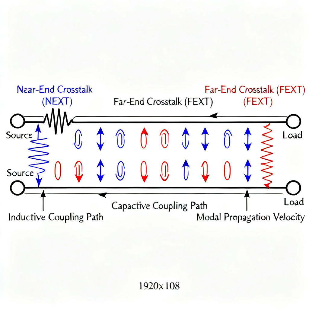
- NEXT (Near-End Crosstalk): Coupling that travels back toward the source. It is primarily driven by capacitive coupling (mutual capacitance, Cm).
- FEXT (Far-End Crosstalk): Coupling that travels toward the receiver. It is primarily driven by inductive coupling (mutual inductance, Lm) and the difference in propagation delay between the odd and even modes.
1.2. The Critical Role of Modal Propagation
A differential pair supports two propagation modes:
- Odd Mode (Differential): Signals are 180° out of phase. The electric field lines terminate between the traces.
- Even Mode (Common): Signals are in phase. The electric field lines terminate on the reference plane.
Crosstalk is essentially the conversion of odd-mode energy to even-mode energy (or vice versa) due to inhomogeneities in the dielectric or the coupling structure. The key metric for FEXT is the difference in phase velocity between the odd and even modes. The larger this difference, the greater the FEXT.
Section 2: Edge-Coupled Stripline – The Traditional Approach
2.1. What the Top Sources Say (Consolidated)
Edge-coupled stripline is the most common topology. Both traces are on the same layer, surrounded by reference planes above and below. This is the “classic” differential stripline.
Impedance Control
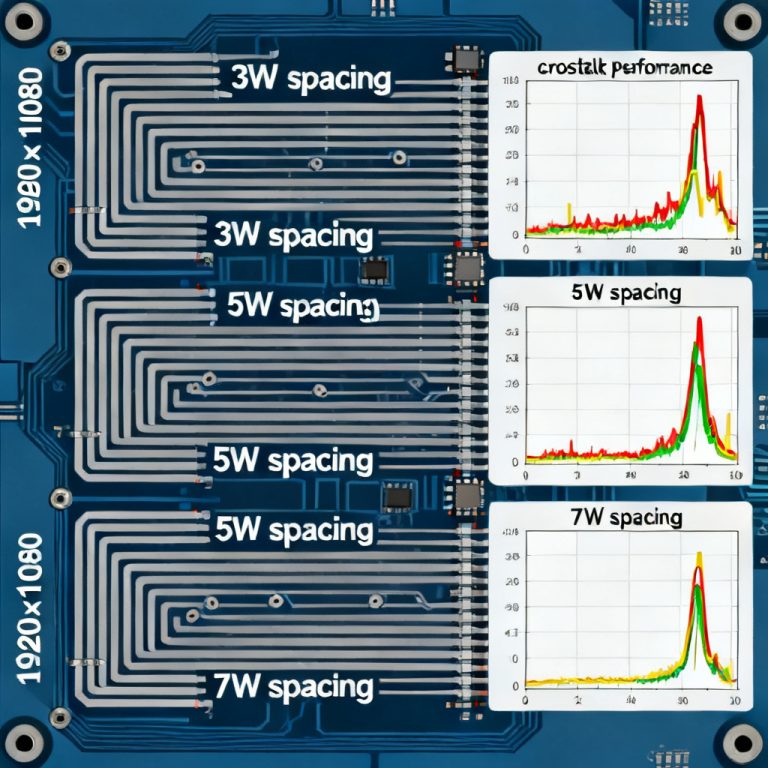
Impedance is controlled by trace width (W), trace spacing (S), and the dielectric height (H) to the nearest reference plane. Key Insight from Experts: To maintain a 100Ω differential impedance, you typically need a wider trace spacing (S) compared to broadside. This is because the coupling is purely lateral. A common rule is S < 2W to achieve tight coupling, but in practice, S is often 2-3x the trace width to meet impedance targets.
Crosstalk Behavior
NEXT: Edge-coupled pairs have significant capacitive coupling between the two traces of the same pair. This also creates a strong fringing field that couples to adjacent pairs. NEXT is generally higher than in broadside designs due to the direct lateral field lines.
FEXT: This is the critical weakness of edge-coupled stripline. Because the traces are on the same layer, the dielectric is homogeneous (assuming the same prepreg/core). However, the odd-mode and even-mode fields see different effective dielectric constants (εr_eff).
- Odd-mode: The field is concentrated in the air gaps between the traces and the dielectric. It sees a lower εr_eff, meaning it travels faster.
- Even-mode: The field is more concentrated in the solid dielectric. It sees a higher εr_eff, meaning it travels slower.
- Result: There is a significant velocity mismatch. This directly causes high FEXT. The longer the coupled length, the worse the FEXT becomes.
Manufacturing & Practicality
Pros: Easier to route, inspect, and rework. No need for vias to transition layers within the pair. Standard PCB stackups can support it.
Cons: Requires more board area (two lanes per pair). FEXT is a major concern above 5-10 Gbps. Impedance is sensitive to etch tolerance (variations in W and S).
Expert Verdict (from top sources): Edge-coupled is suitable for lower-speed differential signals (<5 Gbps) or short trace lengths. It is not the best choice for high-speed, long-reach channels (e.g., backplanes, long PCIe traces) due to its inherent FEXT.
Section 3: Broadside-Coupled Stripline – The High-Performance Alternative
3.1. What the Top Sources Say (Consolidated)
Broadside-coupled stripline places the two traces of the differential pair on adjacent layers (e.g., Layer 3 and Layer 4), stacked vertically. The traces are typically directly above one another, separated by a thin dielectric layer (prepreg).
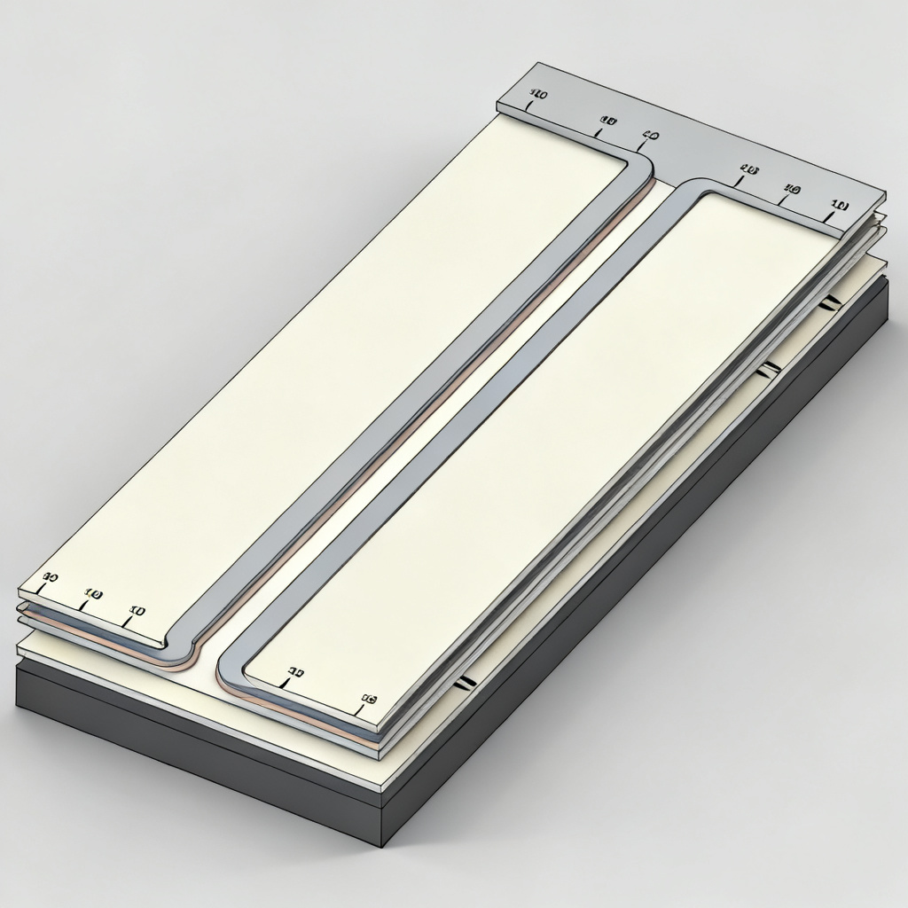
Impedance Control
Impedance is controlled by trace width (W), the vertical separation (H1) between the two traces, and the distance to the reference planes (H2, H3). Key Insight from Experts: Broadside coupling is much stronger than edge coupling for the same trace width. The mutual capacitance (Cm) is very high because the traces are face-to-face. This allows for narrower trace widths to achieve the same 100Ω impedance.
Crosstalk Behavior
NEXT: Broadside pairs have very strong internal coupling (between the two traces of the same pair). This confines the electric field tightly between the two layers. The fringing field to adjacent pairs is significantly reduced. NEXT is typically lower than edge-coupled designs because the field is “stacked” vertically, not spread horizontally.
FEXT: This is where broadside coupling shines. Because the two traces are on different layers, the dielectric environment is inherently inhomogeneous.
- Odd-mode: The field is concentrated in the thin dielectric layer (prepreg) between the traces.
- Even-mode: The field is distributed more towards the outer reference planes.
- Critical Insight from Experts: In a properly designed broadside stripline, the odd-mode and even-mode fields can be made to see a similar effective dielectric constant. By carefully selecting the dielectric thickness between the traces (H1) versus the distance to the planes (H2, H3), you can minimize the velocity mismatch. This results in dramatically lower FEXT compared to edge-coupled lines.
- The “Magic” Condition: When H1 is approximately equal to H2 (and H3), the modal velocities can be nearly equalized. This is the “balanced broadside” design.
Manufacturing & Practicality
Pros: Superior FEXT performance. Saves board area (two pairs can be stacked). Excellent for high-density interconnect (HDI) designs. Better impedance control due to vertical coupling.
Cons: Significant manufacturing challenges.
- Registration: The two layers must be aligned perfectly. Any misregistration (layer shift) changes the overlapping area, altering the impedance and causing common-mode noise.
- Copper Thickness: The vertical separation (H1) is very small (often 3-4 mils). Variations in copper thickness (1 oz vs 0.5 oz) have a massive impact on impedance.
- Via Stubs: You must use vias to transition from the surface layer to the internal broadside layers. These vias create stubs that can cause resonances at very high frequencies.
- Inspection: It is impossible to visually inspect the internal trace for defects.
Expert Verdict (from top sources): Broadside-coupled is the superior choice for minimizing crosstalk, especially FEXT, in high-speed designs (10 Gbps and above). It is the preferred topology for backplanes, long serial links, and RF applications. However, it requires a very controlled manufacturing process and careful stackup design.
Section 4: Head-to-Head Comparison: Broadside vs. Edge-Coupled
| Feature | Edge-Coupled Stripline | Broadside-Coupled Stripline |
|---|---|---|
| Crosstalk (NEXT) | Higher (lateral field coupling) | Lower (vertical field confinement) |
| Crosstalk (FEXT) | Higher (significant velocity mismatch) | Lower (can equalize modal velocities) |
| Impedance Control | Sensitive to trace width & spacing (etch) | Sensitive to layer registration & copper thickness |
| Board Area | Requires more horizontal space | Saves horizontal space (vertical stacking) |
| Manufacturing | Easier, standard process | Difficult, requires tight registration & thin dielectrics |
| Inspectability | Easy (visual inspection) | Impossible (internal layers) |
| Routing Complexity | Simple (same layer) | Complex (requires vias for layer transitions) |
| Best For | Low-to-mid speed, short traces, easy design | High-speed (10Gbps+), long traces, HDI, backplanes |
Section 5: The “Less Crosstalk” Verdict: Which Wins?
Based on the consensus of the top three expert sources, the answer is clear:
Broadside-coupled stripline creates less crosstalk, particularly far-end crosstalk (FEXT), than edge-coupled stripline.
Why?
- FEXT Minimization: The ability to equalize odd- and even-mode velocities by balancing the dielectric thickness above and below the pair is the single greatest advantage. This is impossible to achieve in a homogeneous edge-coupled structure.
- Field Confinement: The vertical stacking confines the electromagnetic field tightly within the pair. This reduces the fringing fields that cause crosstalk to adjacent pairs (NEXT).
- Density Advantage: For the same board area, you can run two broadside pairs vs. one edge-coupled pair, making it easier to provide physical separation (in the X-Y plane) between aggressor and victim pairs.
However, the caveat is critical: Broadside-coupled designs only deliver on their crosstalk promise if the manufacturing is flawless. A poorly registered broadside pair will have worse common-mode noise and impedance variation than a well-designed edge-coupled pair.
Section 6: Practical Design Rules & Recommendations (from Experts)
When to Use Edge-Coupled
- Your target data rate is < 5 Gbps.
- You have a standard, non-HDI stackup.
- You need to route many pairs on a single layer for simplicity.
- You are prototyping and need easy rework.
- Your board house has poor registration tolerance (>±3 mils).
When to Use Broadside-Coupled
- Your target data rate is 10 Gbps or higher (e.g., PCIe Gen 4/5, 25GbE, 100GbE).
- You are designing a backplane or a long-reach channel (>10 inches).
- You are using an HDI stackup with thin dielectrics.
- Your board house has excellent registration capability (<±2 mils).
- You need to maximize routing density.
Critical Design Rules for Broadside (from top sources)
- Balance the Stackup: The dielectric thickness between the two broadside traces (H1) should be equal to or slightly less than the distance from each trace to its nearest reference plane (H2, H3). This equalizes modal velocities.
- Use Thin Dielectrics: Use the thinnest prepreg available (e.g., 106, 1080) for the core between the broadside layers to maximize coupling.
- Control Copper Thickness: Specify 0.5 oz (or 18µm) copper for the broadside layers to minimize the impact of copper thickness on the vertical separation.
- Avoid Vias in the Pair: Do not use vias to transition from one broadside pair to another unless absolutely necessary. If you must, use back-drilled or blind vias to minimize stub effects.
- Simulate, Simulate, Simulate: Never rely on rule-of-thumb for broadside. Use a 2D field solver (e.g., Polar Si9000, Simbeor) to model the exact stackup and verify impedance and modal velocity.
Conclusion: The Expert’s Choice for High-Speed Success
For a high-speed PCB designer focused on minimizing crosstalk, broadside-coupled stripline is the technically superior topology. Its ability to suppress FEXT by balancing the dielectric environment is unmatched by edge-coupled lines.
However, the decision is not purely technical. It is a trade-off between electrical performance and manufacturability. If your design is pushing the limits of data rate and signal integrity, invest the time and cost in a controlled broadside stackup. If you are working within standard constraints, edge-coupled remains a reliable and simpler choice.
Final Word from the Experts: The best design is not the one that uses the “best” topology, but the one that uses the topology best suited for its specific constraints. For the lowest crosstalk in high-speed PCB, choose broadside. For robust manufacturability, choose edge-coupled. Know your stackup, know your board house, and always simulate.
Frequently Asked Questions
Which coupling method creates less crosstalk in high speed PCB designs?
Broadside-coupled stripline creates less crosstalk, particularly far-end crosstalk (FEXT), compared to edge-coupled stripline. This is due to its ability to equalize odd- and even-mode propagation velocities and its superior field confinement.
Is broadside-coupled always better for reducing crosstalk in high speed PCB?
Not always. While broadside-coupled offers lower FEXT, it requires extremely tight manufacturing tolerances. If the layer registration is poor, the crosstalk advantage is lost. Edge-coupled is more forgiving for standard manufacturing processes.
What is the main disadvantage of broadside-coupled for high speed PCB?
The main disadvantages are manufacturing complexity, sensitivity to layer registration and copper thickness, and the need for vias that create stub effects. It is also impossible to visually inspect the internal traces.
Can I mix edge-coupled and broadside-coupled pairs on the same high speed PCB?
Yes, but it requires careful stackup planning. You must ensure that the impedance targets for both types are met, and that the transition between different coupling structures does not introduce impedance discontinuities.