[rank_math_breadcrumb]
Return path discontinuity (RPD) is a primary cause of EMI EMC problems in high speed PCB designs, directly increasing loop area and common-mode radiation.

1. The Physics of Return Path Discontinuity in High Speed PCB
1.1 What is a Return Path in High Speed PCB?
Every signal on a high speed PCB trace requires a corresponding return current. In optimal designs, this return current flows directly beneath the signal trace on the adjacent reference plane due to skin effect and proximity effect, minimizing loop area and inductance.
1.2 How Return Path Discontinuity Occurs in High Speed PCB Designs
Return path discontinuity in high speed PCB happens when: a signal trace crosses a split in the reference plane; a trace changes layers without a nearby return via; vias or connectors force the return current to detour; or antipads/cutouts in the plane are too large.
1.3 The Loop Area Problem in High Speed PCB
The fundamental radiated emissions equation shows that when RPD occurs in a high speed PCB, loop area increases dramatically. Even a small loop area increase at high frequencies can cause emissions to exceed regulatory limits.
2. How Return Path Discontinuity Manifests as EMI EMC Problems in High Speed PCB
2.1 Common-Mode Radiation from Return Path Discontinuity in High Speed PCB
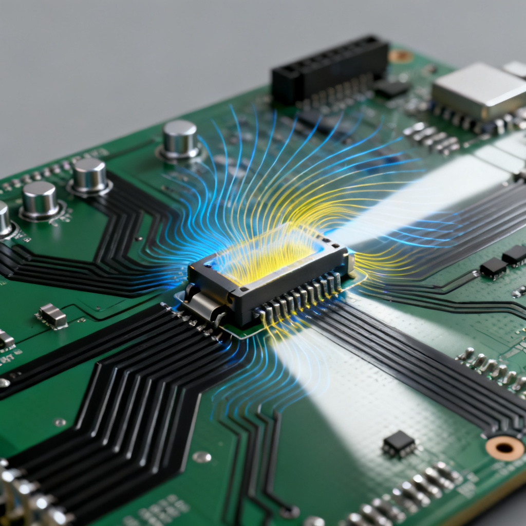
The most direct EMI EMC problem from RPD in high speed PCB is conversion of differential-mode signals into common-mode noise. When the return path is broken, the current flows through external cables or enclosures, acting as an unintentional antenna.
2.2 Ground Bounce and Simultaneous Switching Noise (SSN) in High Speed PCB
Return path discontinuity in high speed PCB also contributes to ground bounce. When multiple signals share a discontinuous return path, their return currents interact, causing voltage fluctuations that corrupt logic levels and increase jitter.
2.3 Increased Crosstalk from Return Path Discontinuity in High Speed PCB
Disrupted return paths in high speed PCB worsen crosstalk between adjacent traces. When a signal’s return current is forced to flow near other traces, it couples into those nets, particularly problematic in dense designs.
3. Real-World Scenarios of Return Path Discontinuity in High Speed PCB
3.1 Split Planes: The Classic Return Path Discontinuity in High Speed PCB
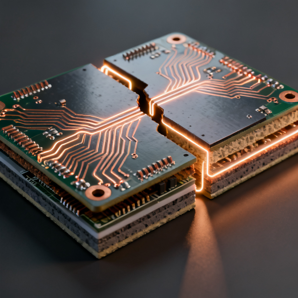
A common high speed PCB design error is using split ground or power planes. If a high-speed trace crosses the split, the return current must travel to the edge of the plane, creating a large loop that radiates strongly.
3.2 Layer Transitions Without Return Vias in High Speed PCB
When a signal changes layers in a high speed PCB without a return via, the return current must travel through plane capacitance or a long path, creating a large loop that increases EMI.
3.3 Connectors and I/O Ports in High Speed PCB
Connectors are notorious for return path discontinuity in EMI/EMC high-speed PCB layouts. If signal and return paths are not closely coupled, the loop area expands, triggering harmful electromagnetic interference and compatibility issues.
4. Mitigation Strategies for Return Path Discontinuity in High Speed PCB
4.1 Never Route High-Speed Signals Across Split Planes in High Speed PCB
This is the golden rule for avoiding return path discontinuity in high speed PCB. If crossing a split is unavoidable, use stitching capacitors or a copper bridge to provide a high-frequency return path.
4.2 Use Return Vias for Layer Transitions in High Speed PCB
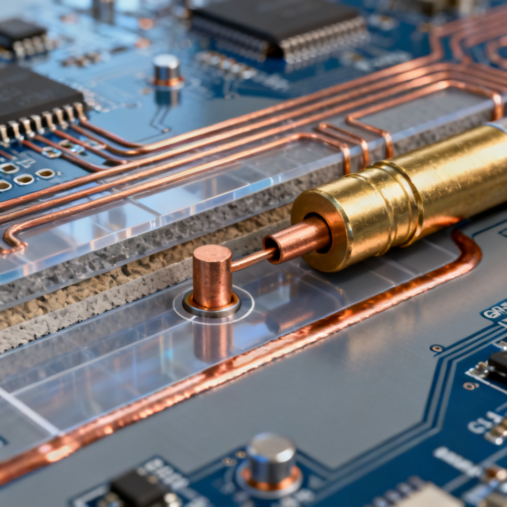
Whenever a signal changes layers in a high speed PCB, place a return via within 1 mm of the signal via to ensure the return current flows directly beneath the signal.
4.3 Optimize Reference Plane Continuity in High Speed PCB
To prevent return path discontinuity in high speed PCB, avoid large antipads around vias, keep ground planes solid under all high-speed traces, and use ground pours on all signal layers.
4.4 Minimize Loop Area in Connectors and Cables for High Speed PCB
Use differential signaling, place ground vias near every signal pin, and use shielded cables to minimize loop area and reduce return path discontinuity effects in high speed PCB.
4.5 Simulation and Verification of Return Path Discontinuity in High Speed PCB
Use 3D field solvers to visualize return paths, measure common-mode currents, and perform TDR to detect impedance discontinuities caused by return path discontinuity in high speed PCB.
5. Advanced Considerations for Return Path Discontinuity in High Speed PCB
5.1 The Role of Dielectric Material in High Speed PCB
Dielectric constant and dissipation factor affect return current behavior. For high-speed designs above 10 Gbps, use low-loss materials and ensure reference plane continuity to minimize return path discontinuity in high speed PCB.
5.2 Power Integrity and Return Paths in High Speed PCB
Return path discontinuity in high speed PCB is not limited to ground planes. Power planes also serve as return paths. Use plane capacitance with thin dielectric to provide a low-impedance return.
5.3 Differential Pairs and Return Path Discontinuity in High Speed PCB
Differential pairs are not immune to return path discontinuity in high speed PCB. If the pair is not tightly coupled or the reference plane is discontinuous, common-mode conversion still occurs. Always route over a continuous ground plane.
Comparison Table: Split Plane vs. Continuous Plane for Return Path Discontinuity in High Speed PCB
| Parameter | Split Plane (RPD) | Continuous Plane (No RPD) |
|---|---|---|
| Loop Area | Large (10-100 mm²) | Small (0.1-1 mm²) |
| Radiated Emissions at 1 GHz | High (exceeds FCC limits) | Low (within limits) |
| Common-Mode Current | Significant | Minimal |
| Signal Integrity Impact | Degraded (jitter, crosstalk) | Preserved |
| Recommended for High Speed PCB | Not recommended | Strongly recommended |
Conclusion: Return Path Discontinuity is the Root of Many EMI EMC Problems in High Speed PCB
Return path discontinuity in high speed PCB directly increases loop area, generates common-mode radiation, and degrades signal integrity. By understanding the physics, recognizing common failure modes, and applying disciplined layout practices—such as avoiding split planes, using return vias, and minimizing loop areas—you can ensure your designs meet EMC standards and function reliably at multi-gigabit speeds. Key Takeaway: Every high-speed signal is only as good as its return path. Design for continuity, and you design for success.
At our facility, we specialize in high speed PCB manufacturing and custom high-speed PCB production with rigorous impedance control and return path optimization. Our high speed PCB fabrication services include advanced simulation, TDR validation, and compliance with global EMC standards. Whether you need prototype high speed PCB or production quantities, our engineering team ensures every high speed PCB meets your signal integrity requirements.
Frequently Asked Questions About Return Path Discontinuity in High Speed PCB
What is return path discontinuity in high speed PCB?
Return path discontinuity in high speed PCB occurs when the current return path for a high-speed signal is interrupted or forced to take a longer, higher-inductance route, causing EMI EMC problems and signal integrity degradation.
How does return path discontinuity cause EMI EMC problems in high speed PCB?
Return path discontinuity in high speed PCB increases the current loop area, which directly increases radiated emissions. It also converts differential-mode signals into common-mode noise, leading to EMI EMC failures.
How can I mitigate return path discontinuity in my high speed PCB design?
To mitigate return path discontinuity in high speed PCB, avoid routing across split planes, use return vias for layer transitions, keep reference planes continuous, and minimize loop areas in connectors and cables.
What tools can detect return path discontinuity in high speed PCB?
Tools like 3D field solvers (Ansys HFSS, CST), TDR (Time Domain Reflectometry), and spectrum analyzers with current probes can detect return path discontinuity in high speed PCB.
Glossary of Key Terms Related to Return Path Discontinuity in High Speed PCB
- Return Path Discontinuity (RPD): An interruption in the intended path for return current in a high speed PCB, causing EMI EMC problems.
- Common-Mode Current: Unwanted current that flows in the same direction on signal and return paths, often generated by RPD in high speed PCB.
- Loop Area: The physical area enclosed by the signal and return current paths; larger loop areas increase radiated emissions.
- Stitching Capacitor: A capacitor placed across a split plane to provide a high-frequency return path and mitigate RPD.
- Return Via: A via placed near a signal via to connect reference planes and ensure a continuous return path.