Master Power Integrity PCB Simulation for DDR5 Memory Power Rails with this definitive guide. DDR5’s lower voltage and higher current transients demand rigorous PDN design to ensure system stability and signal integrity.

Why DDR5 Demands a New Approach to Power Integrity
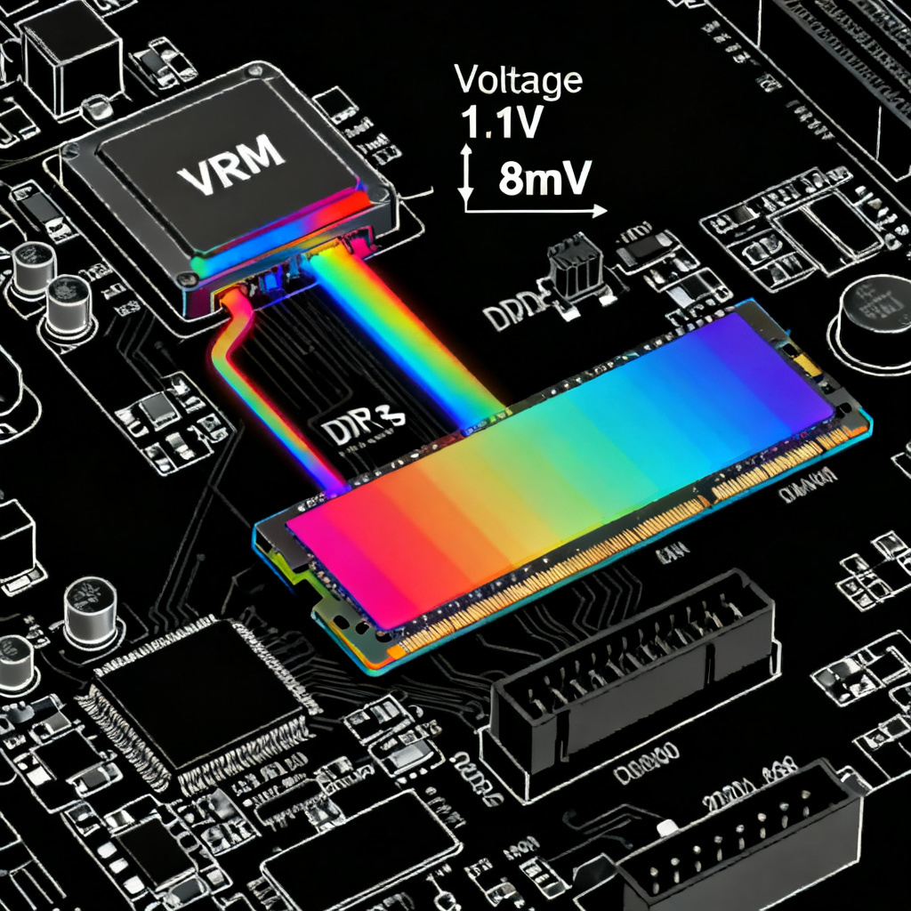
Unlike DDR4, DDR5 introduces critical changes that make Power Integrity PCB Simulation for DDR5 Memory Power Rails non-negotiable. Lower voltage margins (1.1V VDD vs. 1.2V), higher current transients exceeding 5A per channel, and on-module PMIC all increase sensitivity to PDN noise.
Lower Voltage Margins and Higher Current Transients
DDR5’s reduced voltage swing means noise has a proportionally larger impact on signal integrity. A 50mV ripple on a 1.1V rail represents a 4.5% variation, compared to only 3.3% on DDR4. The di/dt is significantly higher, challenging the PDN’s ability to maintain stable voltage.
On-Module PMIC and Increased Crosstalk Sensitivity
The Power Management IC on the DDR5 DIMM regulates local rails, but the motherboard’s PDN must still deliver clean power to the PMIC input. Proximity of power rails to high-speed data lines means any PDN noise can couple into signal paths, degrading the eye diagram.
The Core Simulation Workflow for DDR5 Power Rails
A robust Power Integrity PCB Simulation for DDR5 Memory Power Rails workflow involves three phases: DC Analysis, AC Analysis (Impedance Profile), and Transient Analysis.
DC Analysis: Voltage Drop and Current Density
Ensure the PDN delivers required DC voltage to every load point. For DDR5, analyze 1.1V VDD and 1.8V VPP rails. Target IR drop less than 1% (11mV for 1.1V). Use thicker copper and wider traces for high-current paths. Current density must remain below 30 A/mm².
AC Analysis: Target Impedance and PDN Impedance Profile
Maintain low and flat PDN impedance across a wide frequency range. Calculate Z_target using: Z_target = (VDD × Ripple%) / ΔI. For DDR5 (1.1V, 5% ripple, 3A transient): Z_target = 18.3 mΩ. Control impedance from DC to at least 20 GHz.
Transient Analysis: Time-Domain Voltage Ripple
Transient simulation reveals actual voltage behavior under realistic load conditions. Use piecewise linear current sources mimicking DDR5 burst patterns. Acceptable response: droop < 30mV, overshoot < 20mV, settling time < 50ns.
Critical PCB Design Considerations for DDR5 Power Rails
Simulation is only as good as the design it models. These layout practices are essential for achieving Power Integrity PCB Simulation for DDR5 Memory Power Rails results in the real board.
Power Plane Design
Use solid power and ground layers for 1.1V and 1.8V rails. Minimize dielectric thickness (4-mil) for high-frequency plane capacitance (~100 pF/in²). Avoid plane splits under the DDR5 DIMM area.
Decoupling Capacitor Placement
Place smallest value capacitors closest to DDR5 power pins. Use two vias per capacitor to minimize loop inductance. Keep via length short by placing capacitors on the same side as the power plane.
Return Path and Signal Integrity
For every DDR5 signal via, place a ground via within 100 mils. Ensure signal traces have a continuous reference plane beneath them to reduce crosstalk between power rails and signals.
Advanced Simulation Techniques and Tools
To achieve the highest accuracy, use 3D full-wave EM simulation for frequencies above 1 GHz. Co-simulate with signal integrity to understand PDN impact on jitter. Statistical eye diagram analysis ensures reliable DDR5 operation.
3D Full-Wave EM Simulation
Model exact geometry of vias, planes, and connectors using tools like Ansys HFSS. This captures via stub resonance, anti-pad effects, and plane cavity resonances.
Co-Simulation with Signal Integrity
Feed PDN impedance profile into SI simulation of DDR5 data lanes. This reveals the true impact of PI on SI, ensuring clean eye diagrams.
Statistical Eye Diagram Analysis
Use IBIS-AMI to generate eye diagrams accounting for random jitter and power supply noise. A clean eye opening with height > 200mV and width > 0.3 UI is required.
Common Pitfalls and How Simulation Prevents Them
| Pitfall | Symptom | Power Integrity PCB Simulation Solution |
|---|---|---|
| Insufficient decoupling | Voltage droop during burst reads | Transient simulation reveals missing capacitors at specific frequencies |
| High via inductance | Resonance peak at 50-100 MHz | AC simulation shows peak; add more vias or use larger via diameter |
| Plane resonance | High impedance at 1-2 GHz | 3D EM simulation identifies resonant cavity; add stitching vias |
| Poor capacitor placement | High impedance at 100 MHz | AC simulation with capacitor models shows impact of placement |
| IR drop on VPP rail | Write failures at high temperature | DC simulation identifies bottleneck; widen traces or add copper pours |
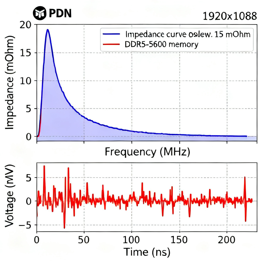
Case Study: Simulating a DDR5-5600 Power Rail
This representative example demonstrates Power Integrity PCB Simulation for DDR5 Memory Power Rails in action. Setup: 8-layer PCB, 2oz copper, Z_target = 15 mΩ, transient load 2A to 6A step in 1ns. Simulation results: DC drop 8 mV, AC impedance below 15 mΩ to 5 GHz, transient droop 28 mV, settling time 40 ns. Eye diagram: height 250 mV, width 0.35 UI—passing DDR5-5600 requirements.
Conclusion and Next Steps
Power integrity simulation for DDR5 memory power rails is a prerequisite for first-pass success. Follow the workflow: DC, AC, transient analysis. Adhere to best practices in plane design and decoupling placement. Partner with experts in high-speed PCB manufacturing to ensure your PDN translates flawlessly from simulation to silicon.
Frequently Asked Questions
What is Power Integrity PCB Simulation for DDR5 Memory Power Rails?
It is the process of analyzing and optimizing the power distribution network to ensure stable voltage delivery to DDR5 memory, using simulation tools to verify PDN impedance, transient response, and decoupling effectiveness.
Why is target impedance important for DDR5 power rails?
Target impedance defines the maximum PDN impedance allowed to keep voltage ripple within acceptable limits. For DDR5, typical Z_target is 15-20 mΩ to prevent data corruption.
How does decoupling capacitor placement affect DDR5 power integrity?
Proper placement minimizes loop inductance and ensures effective decoupling across the frequency range. Small capacitors close to the load handle high-frequency noise, while bulk capacitors near the VRM handle low-frequency transients.
What tools are used for DDR5 power integrity simulation?
Industry-standard tools include Ansys SIwave, Cadence Sigrity, and CST Studio. These enable DC, AC, transient, and 3D EM simulations for comprehensive PDN analysis.
How can I improve DDR5 power rail performance in my PCB design?
Use solid power planes, minimize via inductance, optimize decoupling capacitor values and placement, and perform co-simulation with signal integrity to identify and mitigate noise coupling.
Glossary of Key Terms
PDN (Power Distribution Network): The network delivering power from VRM to loads, including planes, traces, vias, and decoupling capacitors.
Target Impedance (Z_target): The maximum impedance the PDN should present to maintain voltage within specified ripple limits.
IR Drop: Voltage drop across the PDN due to DC resistance, calculated during DC simulation.
Transient Response: The voltage behavior of the PDN under dynamic load changes, such as burst read/write operations.
Decoupling Capacitor: A capacitor placed near the load to provide localized charge storage and reduce PDN impedance at specific frequencies.
Plane Resonance: A resonant condition between power and ground planes that creates high impedance peaks at certain frequencies.
Co-Simulation: Simultaneous simulation of power integrity and signal integrity to analyze their coupled effects on system performance.
Eye Diagram: A graphical representation of digital signal quality, showing voltage and timing margins under noise and jitter.
Via Stub: The unused portion of a via that acts as a resonant stub, causing signal reflections and impedance discontinuities.
EM Simulation: Electromagnetic simulation using full-wave solvers to model high-frequency effects in 3D geometries.
Why Choose Our High-Speed PCB Manufacturing
Our company specializes in manufacturing high-speed, high-layer-count PCBs optimized for DDR5 power integrity. We offer advanced stackup design, precise impedance control, and rigorous simulation validation. Our DFM team works with your simulation results to ensure your PDN translates flawlessly from simulation to silicon. Unlike generic manufacturers, we provide detailed simulation reports and design recommendations to reduce risk and improve first-pass success.