[rank_math_breadcrumb]
Using a near field probe to locate EMI EMC high speed PCB hotspots is a fundamental skill for any engineer designing or troubleshooting modern electronics. This guide provides a complete, step-by-step methodology for identifying electromagnetic interference sources on high-speed printed circuit boards, ensuring compliance and signal integrity.
Core Concepts: Near Field Probes & EMI EMC High Speed PCB Hotspots
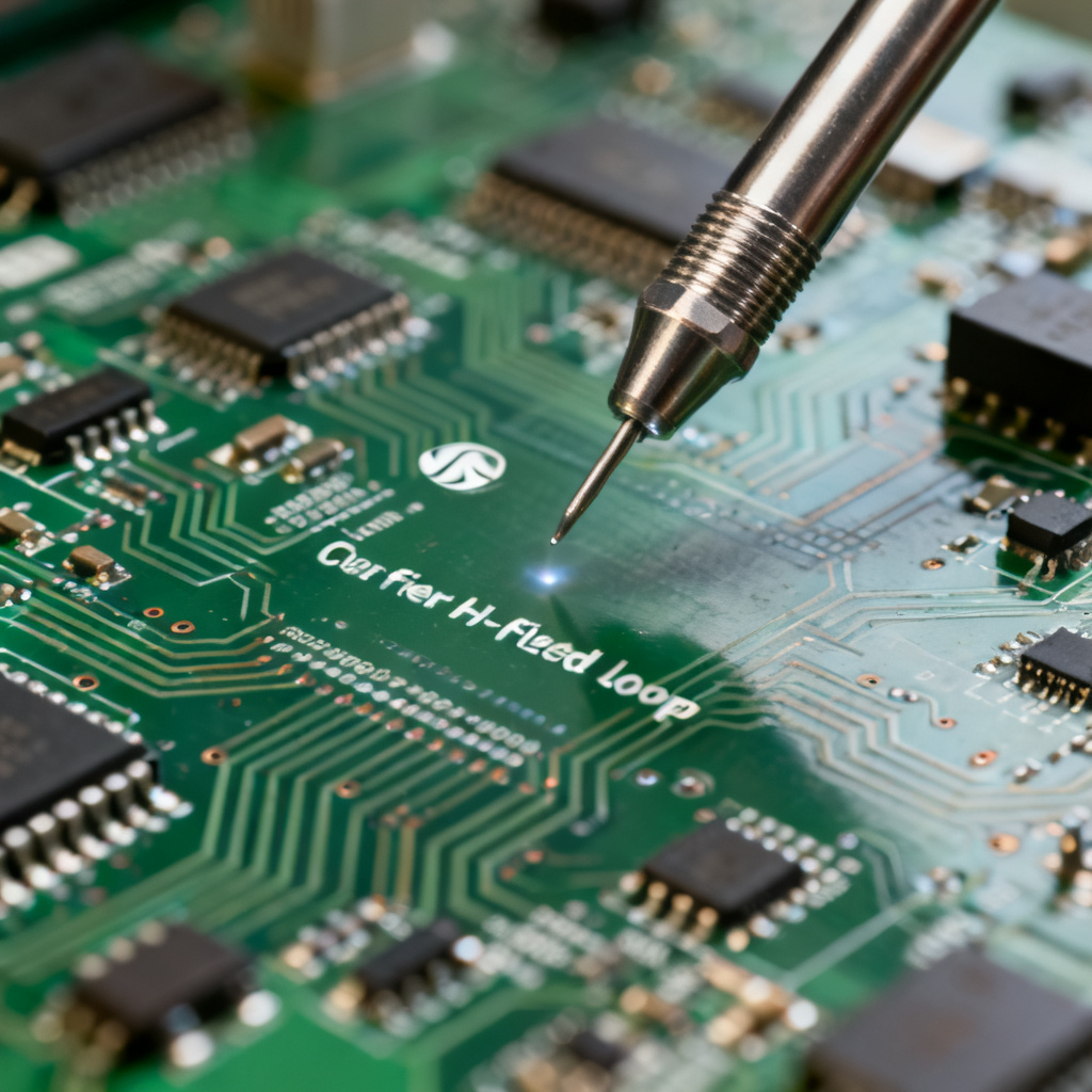
Understanding the fundamentals of near field probing is essential for effective EMI EMC high speed PCB troubleshooting. A near field probe is a passive or active antenna designed to capture magnetic (H-field) or electric (E-field) energy close to a PCB surface. Unlike far-field antennas used in anechoic chambers, near field probes measure the reactive field within a fraction of a wavelength from the source, allowing for precise localization of emissions.
What Is a Near Field Probe?
A near field probe is a small loop or tip connected to a spectrum analyzer or oscilloscope. Common types include:
- Loop Probes (H-field): Best for identifying current loops, trace radiation, and differential-mode noise. They are directional and sensitive to magnetic fields.
- Stub or Tip Probes (E-field): Used for detecting voltage-driven sources, such as IC pins, vias, or high-impedance nodes. They are less directional but helpful for pinpointing electric field coupling.
What Are EMI Hotspots on a High Speed PCB?
EMI hotspots are localized regions where electromagnetic emissions exceed acceptable levels. In high-speed designs, these often occur at:
- High-speed signal traces (e.g., clock lines, data buses) with poor return path design.
- Connector and cable interfaces where common-mode currents couple to external structures.
- IC power pins with inadequate decoupling, causing switching noise to radiate.
- Vias and layer transitions that create impedance discontinuities and radiate energy.
- Ground plane gaps or slots that disrupt return currents.
Step-by-Step Guide: Using a Near Field Probe to Locate EMI EMC High Speed PCB Hotspots
Using a near field probe to locate EMI EMC high speed PCB hotspots requires a structured approach. Follow these steps for reliable results.
Step 1: Choose the Right Probe and Equipment
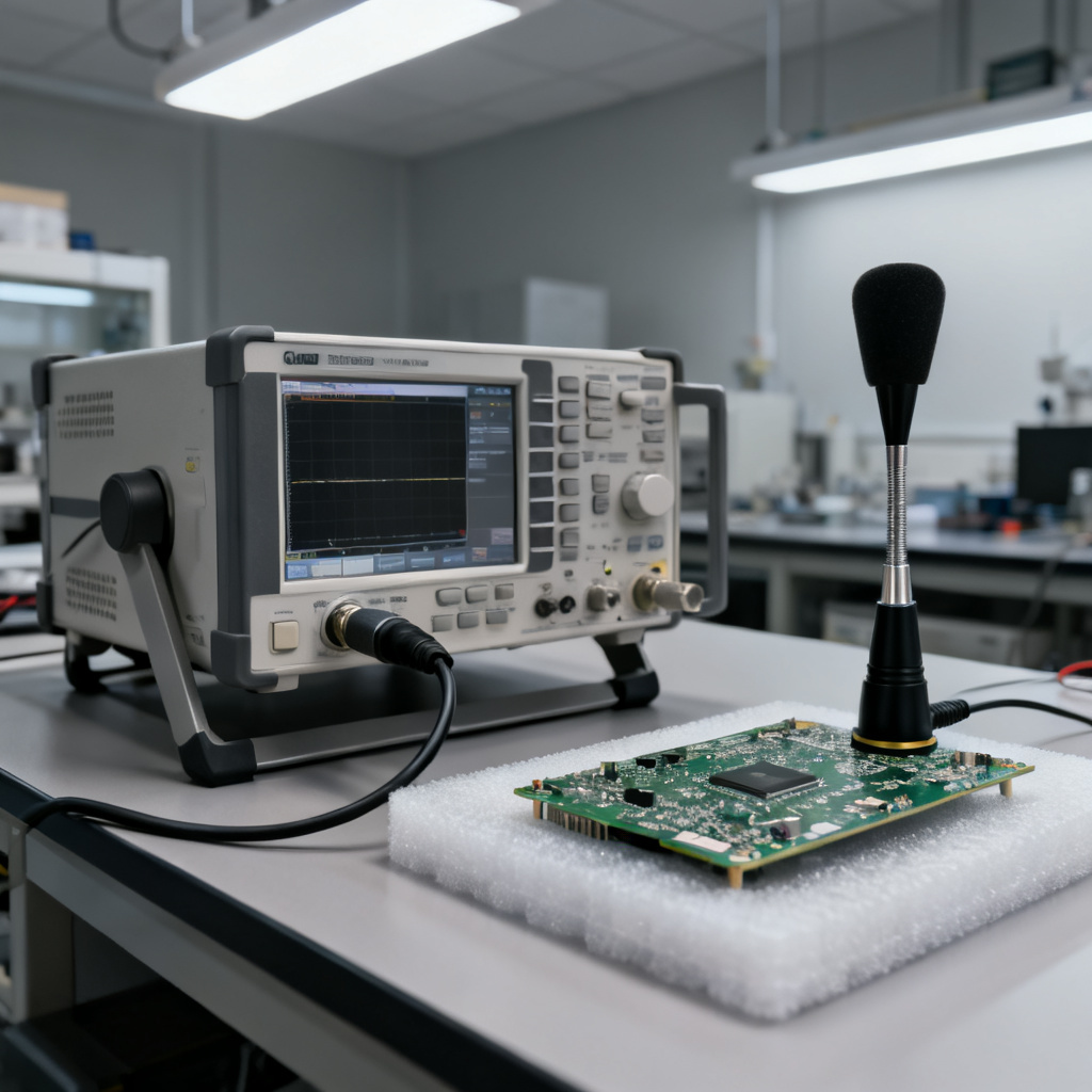
For most high-speed PCB work, start with a magnetic loop probe (e.g., 1 cm or smaller diameter) for general scanning. Use a smaller loop (3-5 mm) for fine localization. An electric field probe is useful for identifying voltage-driven sources, but magnetic probes are more common for current-based emissions. A spectrum analyzer with a tracking generator is ideal for frequency-domain analysis. An oscilloscope with FFT capability works for time-domain correlation. Ensure the probe is calibrated or its transfer factor (dB relative to 1 µV/m or 1 A/m) is known. For weak signals, a low-noise preamplifier (e.g., 20-30 dB gain) can improve sensitivity, but beware of noise floor elevation.
Step 2: Set Up the Test Environment
Place the PCB on a non-conductive, non-reflective surface (e.g., a foam block or wooden table). Avoid metal tables that can distort fields. Use a common ground reference between the probe and spectrum analyzer to reduce noise. Hold the probe perpendicular to the PCB surface for H-field measurements (maximizing loop coupling). For E-field, hold the tip parallel. Maintain a consistent height (e.g., 1-2 mm) using a spacer or fixture for repeatability. Set the spectrum analyzer to cover the fundamental and harmonic frequencies of interest (e.g., 30 MHz to 1 GHz for typical high-speed designs). Use a resolution bandwidth (RBW) of 100 kHz to 1 MHz for initial scans, then narrow to 10 kHz for detailed analysis.
Step 3: Perform a Broadband Scan
Move the probe slowly across the entire PCB surface, observing the spectrum analyzer’s peak trace. Note frequencies where emissions are highest. Common hotspots include near oscillators, clock distribution lines, and power supply areas. Use a marker or pen to label areas where emissions exceed a predefined threshold (e.g., 10 dB above background noise). Document frequency peaks and relative amplitude. Cross-reference hotspots with your PCB layout. For example, a strong emission at 100 MHz might correspond to a 100 MHz clock trace or its harmonics.
Step 4: Localize Specific Hotspots
Switch to a smaller probe (e.g., 3 mm loop) and reduce the scan height to 0.5 mm. Move the probe in a grid pattern (e.g., 1 mm steps) around the suspected area. The probe’s response will peak directly over the source. Use a combination of H-field and E-field probes. If the H-field is strong, the source is likely a current loop (e.g., a trace with poor return path). If the E-field dominates, it’s a voltage node (e.g., an IC pin or via). Optionally, connect the probe to an oscilloscope and trigger on the clock signal. Observe the waveform shape to see if emissions are synchronous with switching events.
Step 5: Analyze and Document Findings
For each hotspot, capture the spectrum trace. Identify whether emissions are narrowband (e.g., clock harmonics) or broadband (e.g., switching noise from power supplies). Narrowband emissions often point to periodic signals; broadband suggests transient events. Create a heatmap of emission intensity using software or manual plotting. This helps visualize the distribution of hotspots across the PCB. Record probe type, position (X-Y coordinates), frequency, amplitude, and any design features (e.g., trace width, via location). This data is crucial for root cause analysis and design iteration.
Interpreting Probe Results: From Hotspot to Root Cause
Effective interpretation of probe data is key to solving EMI EMC high speed PCB issues. Each type of source leaves a distinct signature.
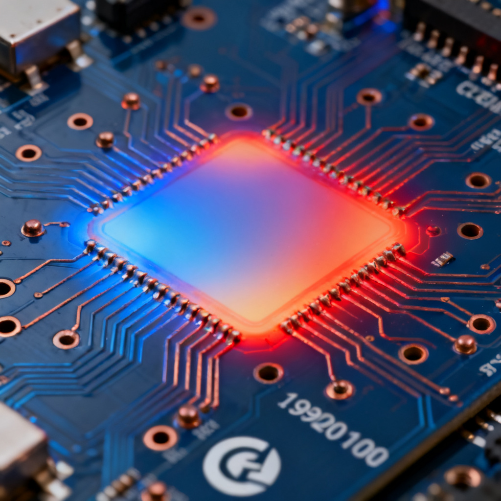
Common EMI Sources and Their Signatures
- Trace Radiation: A narrowband peak at the trace’s fundamental frequency or harmonic, with peak amplitude when the probe is aligned parallel to the trace. Check for inadequate return path (e.g., trace over a split plane) or excessive length.
- Connector Leakage: Broadband noise at connector pins, especially near cable attachment points. This often indicates common-mode currents coupling to the cable shield.
- IC Switching Noise: Broadband emissions near IC power pins, often with a comb-like spectrum (harmonics of the switching frequency). Inadequate decoupling or poor power integrity is typical.
- Via Radiation: Narrowband peaks at vias, especially if the via transitions between layers with different ground references. This suggests impedance discontinuity.
- Ground Plane Issues: Emissions over ground plane slots or gaps, often with a peak at the slot’s resonant frequency. This can occur in mixed-signal designs with split planes.
Differentiating Differential vs. Common-Mode Emissions
Differential-mode emissions show a strong H-field near the trace loop, with emissions proportional to loop area. Use a loop probe to measure the magnetic field around the trace pair. Reducing loop area (e.g., by moving traces closer) mitigates this. Common-mode emissions show a strong E-field near cables or large structures, with emissions independent of trace geometry. Use an E-field probe near connectors or heat sinks. Common-mode chokes or improved grounding are solutions.
Mitigation Strategies for High-Speed PCB Hotspots
Once hotspots are identified using a near field probe, apply targeted fixes to resolve EMI EMC high speed PCB issues.
| Mitigation Strategy | Description | Application for EMI EMC High Speed PCB |
|---|---|---|
| Improve Return Path Design | Ensure every signal trace has a continuous, low-impedance return path (e.g., solid ground plane). Avoid split planes under high-speed traces. Add stitching vias at layer transitions. | Reduces loop area and trace radiation. |
| Optimize Decoupling | Place decoupling capacitors (e.g., 0.1 µF and 10 nF) as close as possible to IC power pins. Use multiple vias to minimize inductance. Consider ferrite beads for high-frequency noise. | Minimizes IC switching noise hotspots. |
| Reduce Loop Area | Route high-speed signals as differential pairs with tight coupling. Use microstrip or stripline geometries with controlled impedance. | Reduces differential-mode emissions. |
| Shield Sensitive Areas | Add grounded copper pours or shielding cans around oscillators, PLLs, or other noise sources. Ensure the shield has low-impedance ground connections. | Contains radiated emissions from localized sources. |
| Filter Connectors | Use common-mode chokes, ferrite cores, or filtering capacitors on I/O lines. Ensure cable shields are grounded at both ends or via a 360-degree termination. | Suppresses common-mode noise at cable interfaces. |
| Manage Layer Transitions | Minimize via usage for high-speed signals. When vias are necessary, use ground return vias adjacent to signal vias to maintain return path continuity. | Reduces via radiation and impedance discontinuities. |
| Use Spread Spectrum Clocking (SSC) | For clock sources, enable SSC to spread energy over a wider frequency band, reducing peak emissions. | Lowers peak amplitude at clock harmonics. |
Advanced Techniques and Best Practices
Mastering near field probing for EMI EMC high speed PCB analysis involves advanced methods to increase accuracy and efficiency.
Using a Near Field Probe with a Preamp or Tracking Generator
A preamp boosts weak signals but can introduce noise. Use a low-noise preamp with a gain of 20-30 dB. Calibrate the system by measuring the noise floor without the DUT. If your spectrum analyzer has a tracking generator, connect it to the probe and use it as a stimulus to identify resonant structures (e.g., cavity resonances in enclosures). This is useful for complex boards.
Combining Near Field and Far Field Measurements
Near field results can predict far field emissions if the source geometry is known. Use the relationship: Far field strength (E) = (I * A * f^2) / (r * c^2), where I is current, A is loop area, f is frequency, r is distance, and c is speed of light. This helps estimate compliance with FCC/CE limits. Near field probing is not a substitute for full far field testing but is excellent for pre-compliance debugging. Address hotspots before sending to a test lab to save time and cost.
Common Pitfalls to Avoid
- Probe Loading: The probe can disturb the field, especially for E-field measurements. Use a high-impedance probe (e.g., 1 MΩ) and keep the probe small.
- Ambient Noise: Background RF (e.g., Wi-Fi, cell signals) can mask emissions. Use a shielded enclosure or conduct tests in a quiet environment.
- Incorrect Probe Orientation: For H-field, the loop must be perpendicular to the current flow. Rotate the probe 90 degrees to check for maximum response.
- Ignoring Near Field to Far Field Conversion: A strong near field hotspot may not always translate to a far field failure. Use analytical models or simulation software to estimate far field levels.
Case Study: Debugging a High-Speed Clock Hotspot
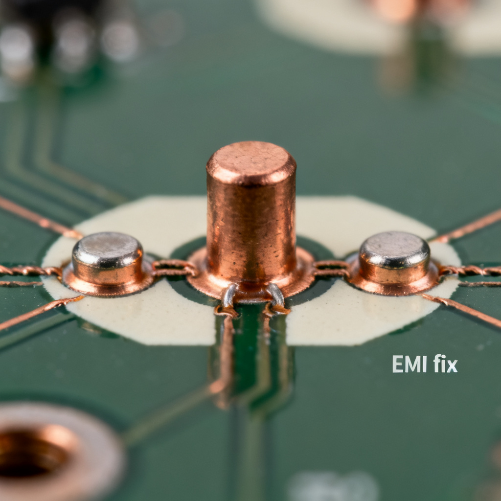
Scenario: A 100 MHz clock line on a 4-layer PCB failed FCC Class B radiated emissions at 300 MHz (third harmonic). Near field probing identified a hotspot at a via where the clock trace transitioned from top to bottom layer.
Steps:
- Scan: Using a 5 mm loop probe, the peak emission was found directly over the via. The spectrum showed a narrowband peak at 300 MHz.
- Root Cause: The via had no ground return via nearby, causing a large current loop between the top and bottom ground planes.
- Fix: Added two ground vias adjacent to the signal via (within 2 mm). The hotspot amplitude dropped by 15 dB.
- Verification: Re-scan showed no residual hotspot. Far field pre-compliance testing passed.
Conclusion: Integrating Near Field Probing into Your Design Workflow
Using a near field probe to locate EMI EMC high speed PCB hotspots is a skill that combines theoretical knowledge with practical technique. By mastering probe selection, scanning methodology, and interpretation of results, you can dramatically reduce design iterations and improve first-pass success rates. For B2B PCB manufacturers and designers, this capability is invaluable—it ensures your high-speed boards meet regulatory standards and perform reliably in the field.
Next Steps: Invest in a quality near field probe kit (e.g., from Tekbox, Langer, or Rohde & Schwarz). Practice on a known noisy board to build confidence. For complex designs, consider combining near field probing with simulation tools (e.g., CST, ANSYS HFSS) for a holistic EMC strategy.
FAQ: Near Field Probe for EMI EMC High Speed PCB
What is the best probe for locating EMI hotspots on a high speed PCB?
A magnetic loop probe (H-field) is typically the best choice for initial scanning of EMI EMC high speed PCB hotspots due to its sensitivity to current loops and trace radiation.
How do I set up a spectrum analyzer for near field probing?
Set the frequency range to cover the fundamental and harmonics of your high-speed signals, use a resolution bandwidth of 100 kHz to 1 MHz for initial scans, and ensure proper grounding to reduce noise.
Can near field probing replace anechoic chamber testing?
No, near field probing is a pre-compliance tool for identifying and mitigating EMI EMC high speed PCB issues before full far field testing in an anechoic chamber.
Internal Links: High-Speed PCB Design Guide | EMC Compliance Checklist | Contact Our Engineering Team for Custom PCB Solutions
External References: FCC Part 15 Guidelines | IEC 61000-4-20 EMC Standards