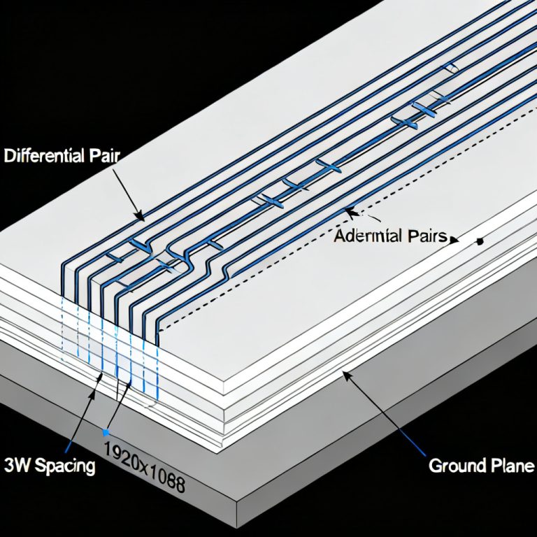
In high-speed PCB design, a return path discontinuity is a primary source of deterministic jitter that degrades timing margin. This article explains the physics of current loops, impedance mismatches, and mode conversion, providing a clear understanding of why a continuous return path is essential for signal integrity in your high-speed PCB.
Fundamental Physics: Current Loops and the Return Path
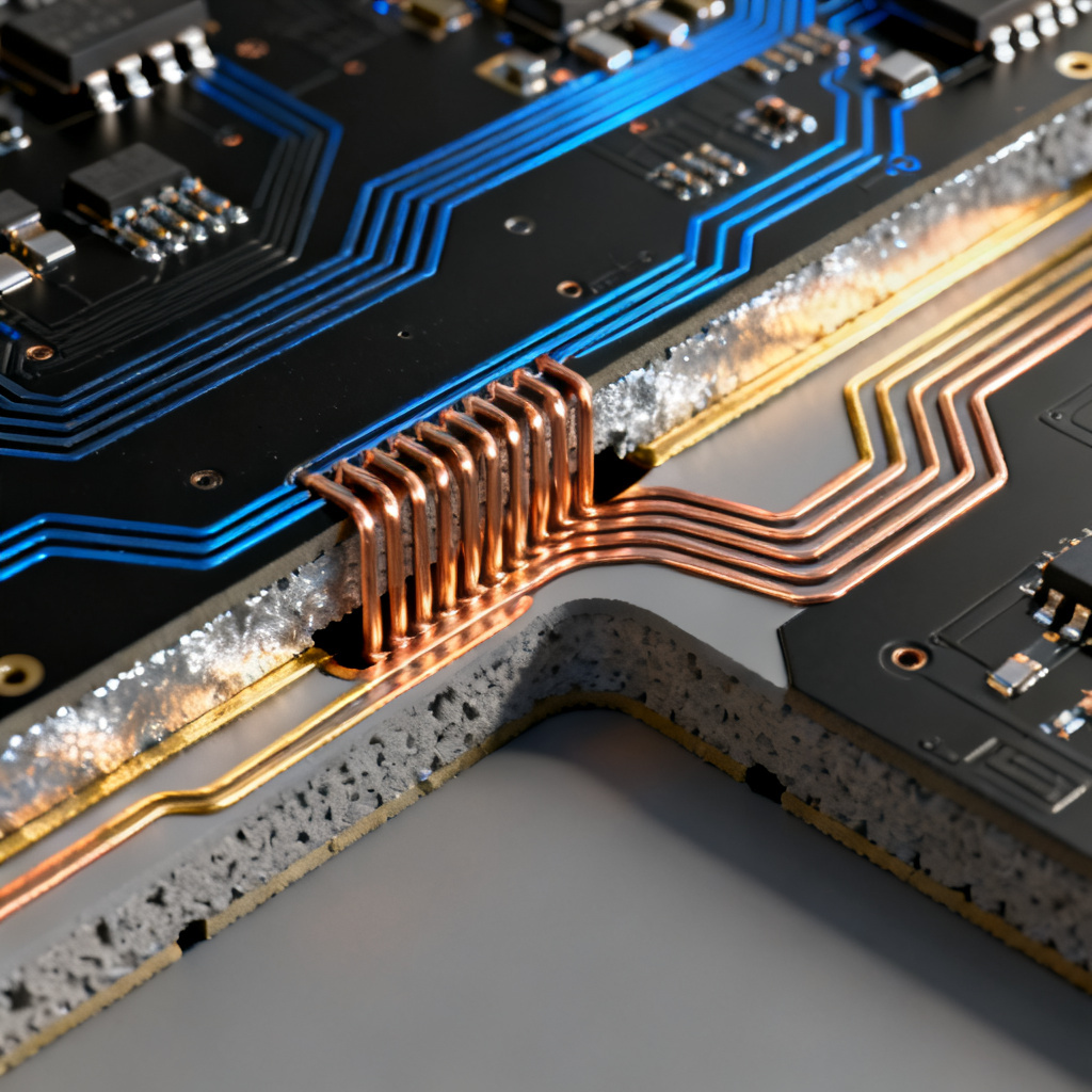
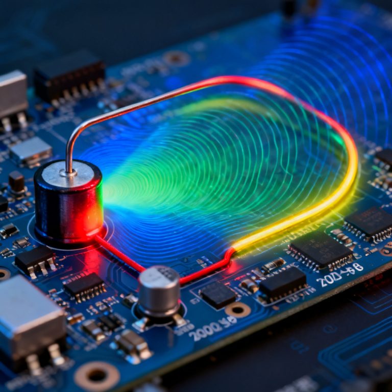
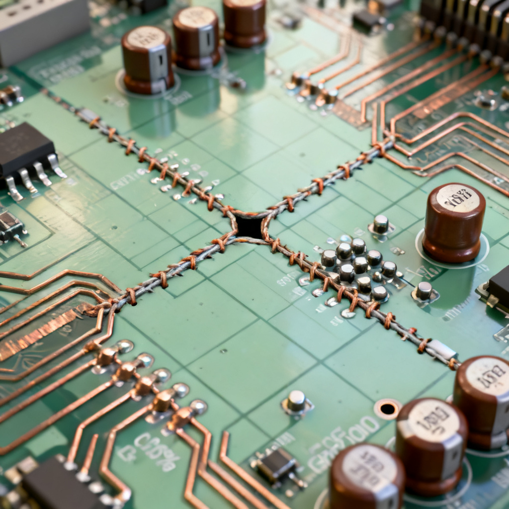
A return path discontinuity occurs when the high-frequency return current is forced to deviate from its natural path directly under the signal trace. At high frequencies, the return current concentrates beneath the trace due to the proximity effect, creating a tightly coupled low-inductance loop. Common causes of return path discontinuity include split ground planes, gaps or moats in the reference plane, via transitions, and connector pin fields where the reference plane is absent.
When the return current is blocked, it must find an alternative longer path, introducing excess loop inductance. This fundamental principle drives the entire jitter generation mechanism in your high-speed PCB.
How Return Path Discontinuity Generates Jitter: The Two-Part Mechanism
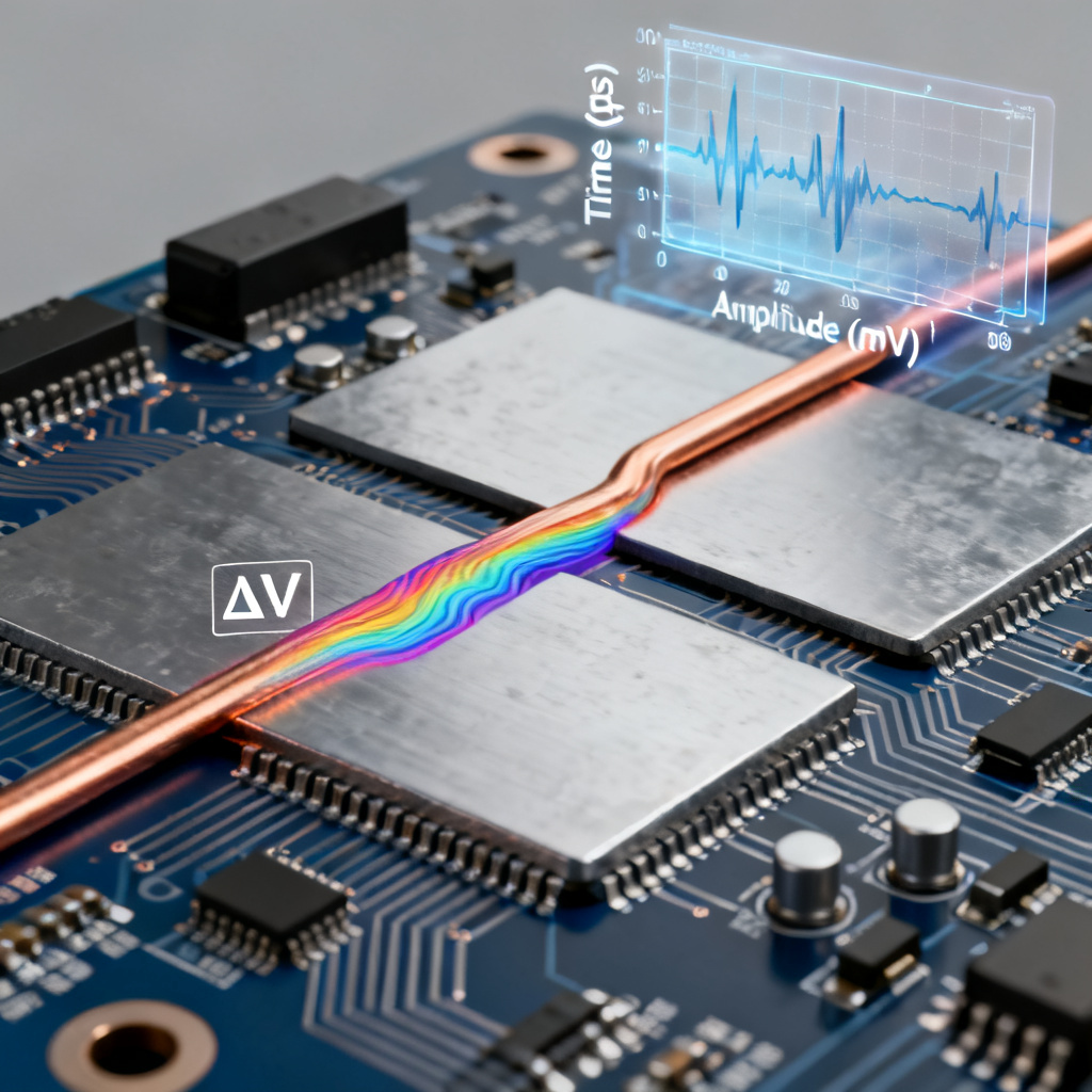
The generation of jitter from a return path discontinuity is a two-step process: first a voltage drop is created, then this voltage drop corrupts the signal’s timing.
Step 1: The Voltage Drop (ΔV)
The excess loop inductance (L_excess) caused by the detoured return path acts as a parasitic element. As the signal’s rising or falling edge drives a changing current (dI/dt) through this inductance, a voltage drop (ΔV) is generated across it: ΔV = L_excess × (dI/dt). This ΔV is a ground bounce or reference voltage shift that physically lifts the local ground potential at the discontinuity point relative to the driver’s ground.
Step 2: The Timing Error (Jitter)
The receiver determines the signal’s logic state by comparing the incoming signal voltage against a fixed threshold. A shift in the local ground (ΔV) effectively changes the threshold the receiver sees. The signal now has to travel a different voltage swing to cross the shifted threshold, causing the crossing point to occur earlier or later than expected. This variation in crossing time is jitter. The magnitude of ΔV depends on the dI/dt of the specific data bit, making the jitter data-dependent and deterministic (DJ), specifically Duty Cycle Distortion (DCD) or Data-Dependent Jitter (DDJ).
Key Insight: The jitter magnitude is directly proportional to the rate of change of the current (dI/dt). Faster edge rates generate significantly more jitter from the same return path discontinuity than slower edge rates.
The Critical Role of Mode Conversion
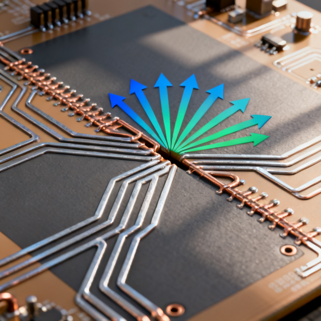
A deeper effect of a return path discontinuity is mode conversion. In a perfect transmission line, the signal propagates in the differential mode. A return path discontinuity forces a portion of this energy to convert into the common mode. The detoured return current now flows on the edges of the split plane or via the chassis as common-mode current. These common-mode currents are highly efficient antennas that radiate electromagnetic interference (EMI) and couple into adjacent traces, creating additional noise and jitter, which appears as eye diagram closure and reduced timing margin in high-speed serial links. The detour path itself forms a resonant cavity that at specific frequencies can amplify the ΔV and resulting jitter, explaining why a return path discontinuity can cause peaking in the jitter versus frequency plot.
Quantifying the Jitter: From Theory to Reality
The jitter (J) from a return path discontinuity can be approximated by: Jitter (ps) ≈ (L_excess × dI/dt) / (Slew_Rate). For a practical example with a 1.8V CMOS signal having a slew rate of 2V/ns, a driver with 50Ω output impedance creating dI/dt of 40 mA/ns, and a 5 mm gap in the ground plane creating L_excess of approximately 1 nH, the jitter is approximately 20 ps. This is significant for a 1 Gbps signal where the unit interval is 1000 ps. In a system with multiple discontinuities such as vias, connectors, and splits, the jitter can quickly accumulate and close the timing budget.
Mitigation Strategies: Designing for a Continuous Return Path
The best way to eliminate return path discontinuity induced jitter is to prevent the discontinuity. Here are the top strategies:
| Mitigation Strategy | Return Path Discontinuity Type Addressed | Implementation Detail |
|---|---|---|
| Solid uninterrupted reference planes | All types | Use a contiguous ground plane as primary reference; avoid splits or gaps |
| Stitching capacitors for plane splits | Split ground planes | Place 0.1 µF or 0.01 µF capacitor bridging the two planes near the signal crossing |
| Ground vias for layer transitions | Via transitions | Place ground via within 50-100 mils of the signal via |
| Return path vias at connectors | Connector pin fields | Place multiple ground stitching vias around signal vias |
| Coplanar waveguide with ground | Missing reference plane | Use ground traces on same layer as signal for local return path |
| Keep critical signals away from boundaries | Plane edges and gaps | Route at least 10× dielectric height (10h) away from any plane edge |
Each of these strategies directly reduces the excess loop inductance that causes the voltage drop and subsequent jitter in your high-speed PCB.
Advanced Considerations: Differential Signaling and Return Path
Differential signaling is often thought to be immune to return path issues because the return current flows in the complementary trace. While this is true for the differential-mode component, no pair is perfectly balanced. There is always a small common-mode component that requires a return path through the reference plane. A return path discontinuity will block this common-mode current, generating common-mode noise and jitter. Even for differential pairs, maintain a solid ground plane underneath and use stitching vias for differential vias just as you would for single-ended vias.
FAQ on Return Path Discontinuity and Jitter
What is a return path discontinuity in high speed PCB?
A return path discontinuity is any interruption in the continuous low-impedance path that high-frequency return current needs to follow directly beneath the signal trace. Common examples include split ground planes, gaps in the reference plane, via transitions between layers, and connector pin fields without proper grounding.
How does return path discontinuity generate jitter?
A return path discontinuity creates excess loop inductance that generates a voltage drop (ΔV = L_excess × dI/dt) when the signal switches. This voltage shift changes the receiver’s effective threshold, causing the signal crossing point to occur at different times for different data patterns, producing deterministic jitter.
What is mode conversion and why does it matter?
Mode conversion occurs when a return path discontinuity forces signal energy from the desired differential mode into the common mode. This creates common-mode currents that radiate EMI and couple into adjacent traces, amplifying noise and jitter in the high-speed PCB.
How can I calculate jitter from a return path discontinuity?
Use the formula: Jitter (ps) ≈ (L_excess × dI/dt) / (Slew_Rate). For example, a 1 nH excess inductance with 40 mA/ns current slew rate and 2 V/ns voltage slew rate produces approximately 20 ps of jitter.
What are the best mitigation techniques?
The most effective techniques include using solid uninterrupted ground planes, placing stitching capacitors across plane splits, adding ground vias near signal vias during layer transitions, using multiple stitching vias at connectors, and keeping high-speed signals at least 10× the dielectric height away from plane edges.
Does differential signaling eliminate return path issues?
No. While differential-mode current cancels in the reference plane, the common-mode component still requires a clean return path. A return path discontinuity will block this common-mode current and generate jitter, so even differential pairs need continuous reference planes and proper stitching vias.