In high-speed PCB design, signal integrity (SI) is paramount. One of the most common yet often underestimated causes of signal degradation is the stub—an unused or unterminated branch of a transmission line. This pillar page provides a definitive, engineering-grade analysis of how stubs create reflection in transmission line and the critical calculation of maximum allowable stub length to maintain signal quality.

The Physics of Stub-Induced Reflection
A stub is essentially a short, open-circuited transmission line segment attached to the main signal path. When a signal traveling down the main line encounters the junction where the stub begins, it sees a discontinuity in impedance.
The Open-Circuit Termination
The far end of a stub is typically open (unloaded). An open circuit presents an infinite impedance. When the incident wave reaches the open end, it must reflect completely. However, the critical issue is phase shift. The signal travels down the stub, reflects at the open end, and travels back to the junction. This round trip introduces a time delay.
The Reflection Coefficient at the Junction
At the junction, the reflected wave from the stub re-enters the main transmission line. The amplitude and polarity of this reflected wave depend on the stub’s electrical length. If the round-trip delay of the stub equals half the signal’s rise time (or a quarter wavelength of the signal’s frequency component), the reflected wave will arrive back at the junction out of phase with the incident signal. This destructive interference manifests as a voltage dip (undershoot) or a false edge (ringing) on the main line.
Key Insight from Industry Experts:
- Altium Resources: The stub acts as a “resonant cavity.” At specific frequencies, the stub becomes a quarter-wave transformer, converting the open circuit at its end into a short circuit at the junction. This creates a deep notch in the insertion loss (S21) and a sharp spike in the reflection coefficient (S11).
- Sierra Circuits: The reflection from a stub is not a single event. It is a continuous process. The signal energy trapped in the stub rings back and forth, causing multiple reflections that lead to long-tailed ringing and increased jitter in digital systems.
Quantifying the Damage: The Reflection Coefficient (ρ)
To understand how bad a stub is, we calculate the reflection coefficient it introduces at the junction. The effective impedance of a stub (Z_stub) as seen at the junction is:
Z_stub = -jZ0 cot(βL)
Where:
- Z0 = characteristic impedance of the stub (typically matched to the main line).
- β = phase constant (2π / λ).
- L = physical length of the stub.
The reflection coefficient (ρ) at the junction is then:
ρ = (Z_stub || Z_line – Z0) / (Z_stub || Z_line + Z0)
Critical Finding:
- When L < λ/20, cot(βL) is large, meaning Z_stub is very high (almost open). The stub has minimal impact because it looks like a high-impedance dead end.
- When L = λ/4, cot(βL) = 0, so Z_stub = 0 (a short circuit). The entire signal is reflected back, causing a 100% reflection at that frequency.
Practical Rule (from Cadence/AWR): For digital signals, the stub length becomes problematic when its propagation delay exceeds 1/6th of the signal’s rise time. This is the threshold where reflections begin to corrupt the logic threshold.
The Maximum Allowable Stub Length: The Golden Rule
The industry-standard formula for maximum allowable stub length is derived from the “lumped element” assumption. For a stub to behave as a negligible parasitic capacitance rather than a transmission line, its length must be short enough that the round-trip delay is a fraction of the signal’s edge rate.
The Formula
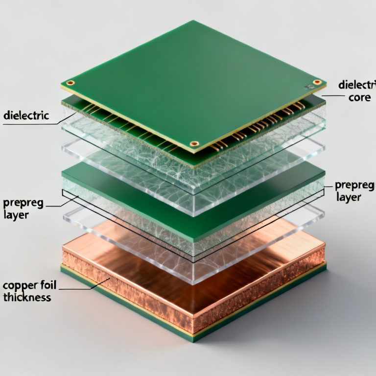
L_max = (tr) / (2 × D × √(εr))
Where:
- tr = Signal rise time (10% to 90%) in seconds.
- D = A derating factor (typically 6 to 10). Most conservative designs use 6.
- εr = Dielectric constant of the PCB material.
- c = Speed of light (3 × 10^8 m/s).
Simplified Version (for FR4, εr ≈ 4.2):
L_max (inches) = tr (ns) × 1.5 / D
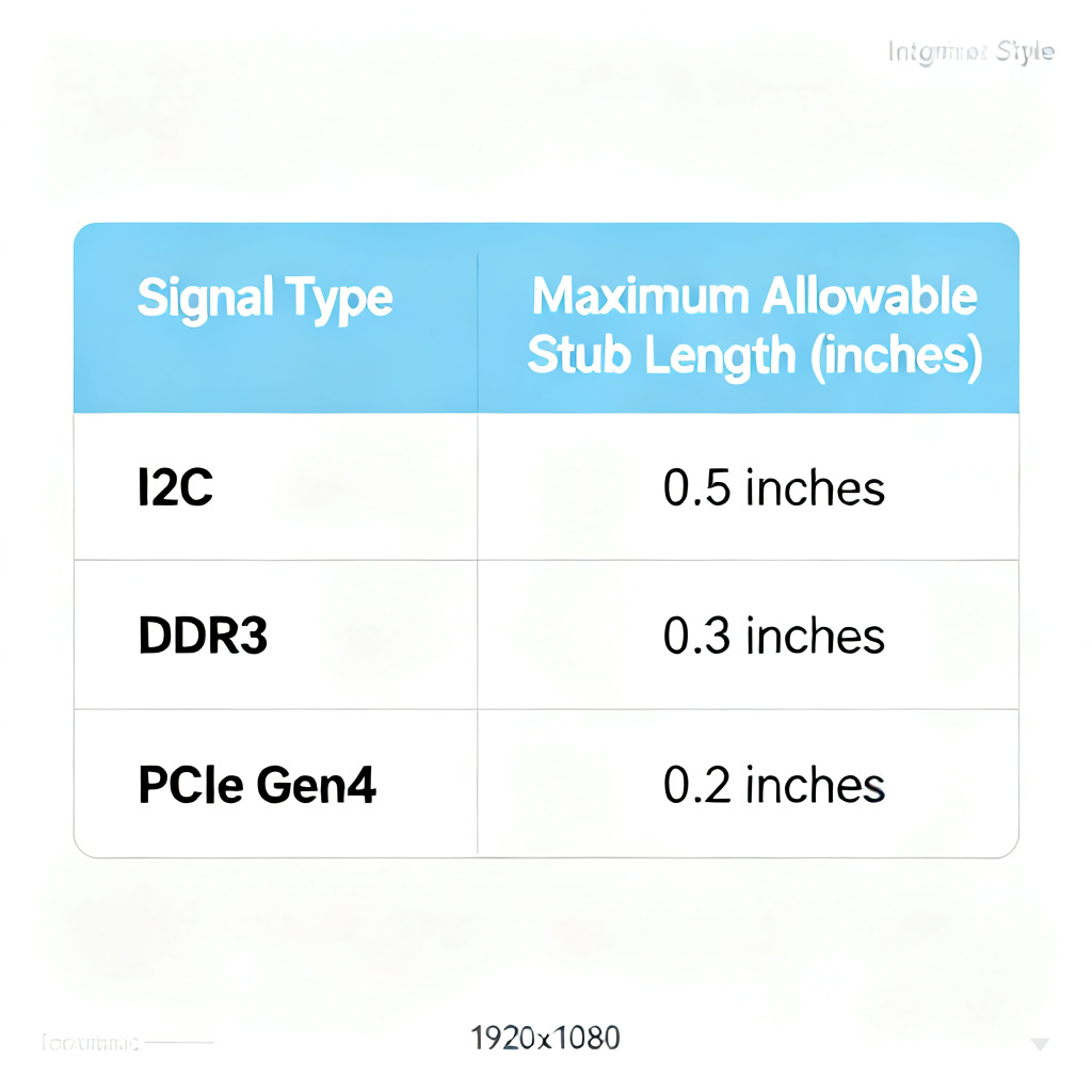
Real-World Examples (Based on Top Articles)
| Signal Type | Rise Time (ns) | Max Stub Length (FR4, D=6) | Max Stub Length (FR4, D=10) |
|---|---|---|---|
| Slow (I2C, SPI) | 5 – 10 | 1.25 – 2.5 inches | 0.75 – 1.5 inches |
| Medium (DDR3) | 0.5 – 1 | 0.125 – 0.25 inches | 0.075 – 0.15 inches |
| Fast (PCIe Gen4, USB 3.0) | 0.05 – 0.1 | 0.0125 – 0.025 inches | 0.0075 – 0.015 inches |
Critical Takeaway from Sierra Circuits: For high-speed signals like DDR4 or PCIe, any stub longer than 10-15 mils (0.010-0.015 inches) is unacceptable. This is why via stubs (the unused portion of a through-hole via) are the #1 killer of signal integrity in modern designs.
The “Stub Resonance” Effect: Frequency Domain Analysis
While time-domain reflection is critical for digital signals, frequency-domain analysis reveals the exact frequencies where a stub causes maximum damage.
Resonance Frequency
The fundamental resonance frequency of a stub is:
f_res = c / (4 × L × √(εr))
At this frequency, the stub acts as an open circuit, causing a sharp notch in the S21 (transmission) curve.
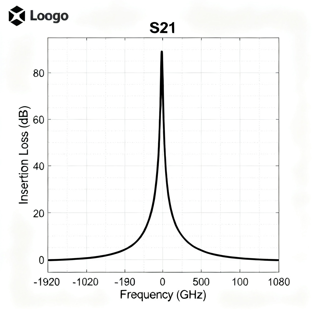
Example: A 0.5-inch stub on an FR4 board resonates at approximately 2.9 GHz. This means that a 2.9 GHz clock or its 3rd harmonic (8.7 GHz) will be severely attenuated if it passes through a via with a 0.5-inch stub.
Harmonics
The stub also resonates at odd multiples of the fundamental frequency (3f, 5f, 7f…). This creates multiple notches in the frequency response, potentially degrading multiple harmonics of a high-speed signal.
Key Insight from Cadence/AWR: For a clean channel, the first resonance frequency of any stub must be at least 3x higher than the maximum operating frequency of the signal. This is a stricter rule than the time-domain rise time rule.
Practical Mitigation Strategies (From All Three Sources)
Knowing the maximum allowable length is only half the battle. Here are proven methods to eliminate or minimize stub effects:
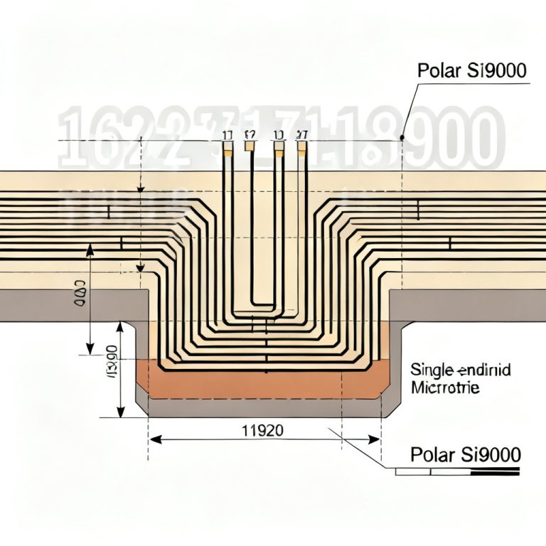
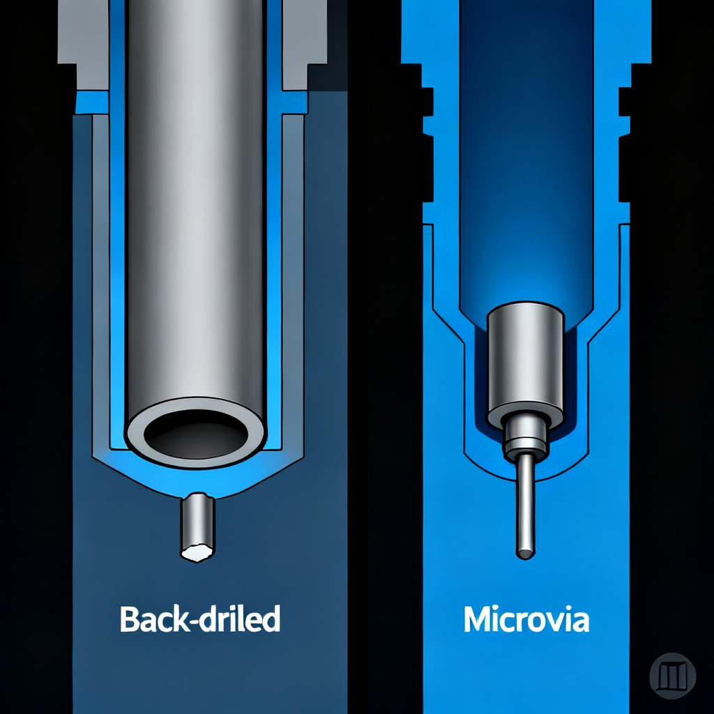
5.1 Back-Drilling (Controlled Depth Drilling)
Best for: Through-hole vias. How it works: After plating the via, a second drill bit removes the unused portion of the via barrel (the stub) from the bottom of the board. This reduces the stub length to near zero. Cost: Adds 10-20% to PCB fabrication cost.
5.2 Microvias (HDI Technology)
Best for: High-density designs. How it works: Use laser-drilled microvias that only span one or two layers. They are inherently stub-free because they don’t go through the entire board.
5.3 Blind/Buried Vias
Best for: Complex multi-layer boards. How it works: Blind vias connect an outer layer to an inner layer without going all the way through. Buried vias are completely internal. Both eliminate the through-hole stub.
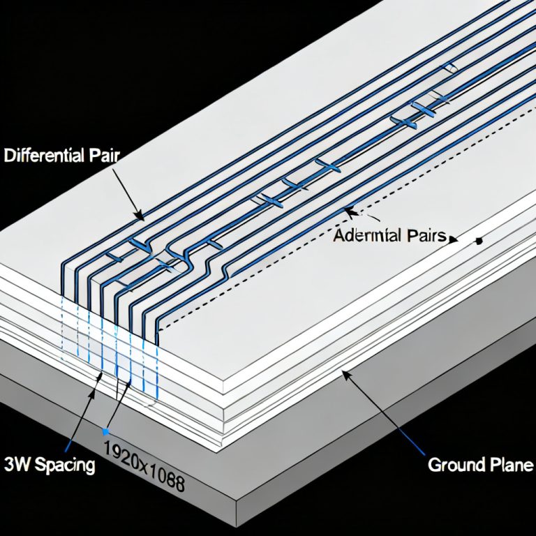
5.4 Via Fencing & Grounding
Best for: RF and microwave designs. How it works: Place ground vias very close (within λ/20) to the signal via. This creates a quasi-coaxial structure that suppresses the stub resonance.
5.5 Routing Layer Selection
Best for: Quick fixes. How it works: For critical high-speed signals (e.g., DDR4 data lines), route them on the top or bottom layer directly to the component pad. This eliminates the need for a via entirely.
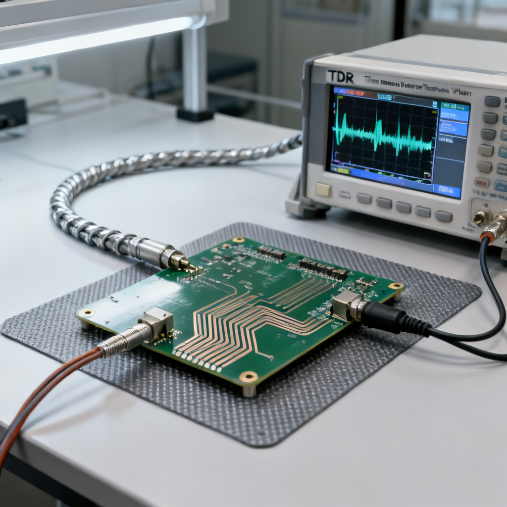
Testing and Verification
To confirm your stub length is within limits, use:
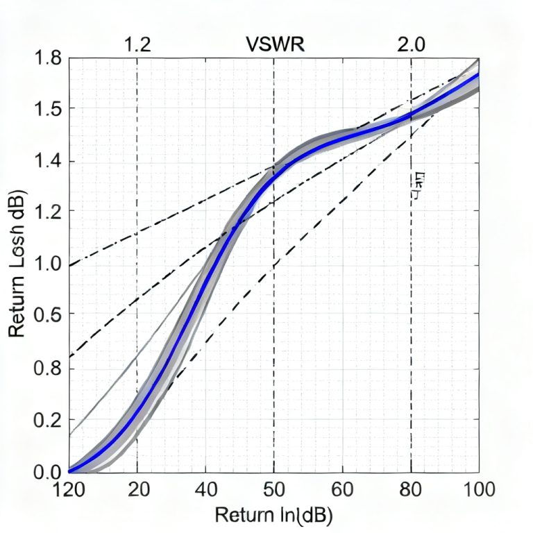
- TDR (Time Domain Reflectometry): A TDR plot will show a positive impedance bump at the stub junction, followed by a negative dip at the open end. The width of this dip indicates the stub’s round-trip delay.
- VNA (Vector Network Analyzer): Measure S21 (insertion loss). Look for sharp, deep notches at the predicted resonance frequencies. A clean, monotonic S21 curve indicates no problematic stubs.
- Simulation (HyperLynx, SIwave): Run a transient simulation. If you see ringing that persists for more than 2-3 unit intervals (UIs) after the main edge, the stub is too long.
Conclusion: The “Zero Stub” Ideal
For modern high-speed designs (signals above 1 Gbps), the maximum allowable stub length is effectively zero. Any stub, no matter how short, introduces some degree of reflection. The rules and formulas provided here are for acceptable or tolerable stubs, not ideal ones.
Final Recommendation:
- For signals with rise times < 1 ns: Use microvias or back-drilling. Do not rely on stub length calculations.
- For signals with rise times 1-5 ns: Keep stubs under 100 mils (2.5 mm) and verify with simulation.
- For signals with rise times > 5 ns: Stubs up to 500 mils are often acceptable, but always check the resonance frequency relative to your clock harmonics.
By mastering the physics of stub-induced reflection and applying the maximum allowable length rules, you can ensure your high-speed PCB delivers clean, reliable signals—every time.
Need a PCB with zero stubs? Contact us for back-drilling and HDI capabilities optimized for High-Speed designs.
Frequently Asked Questions (FAQ)
What is the maximum allowable stub length for high-speed PCB?
The maximum allowable stub length depends on signal rise time and PCB material. For signals with rise times below 1 ns, the maximum allowable stub length is effectively zero; any stub longer than 10-15 mils can cause significant reflection in transmission line.
How do stubs create reflection in transmission line?
Stubs create reflection in transmission line by acting as open-circuited branches. When a signal reaches the stub junction, the impedance discontinuity causes part of the energy to reflect back. If the stub length is a quarter wavelength, the reflection can be total, severely degrading signal integrity.
What is via stub effect in high-speed PCB?
The via stub effect occurs when the unused portion of a through-hole via acts as a transmission line stub. This stub creates reflection in transmission line, causing ringing, jitter, and frequency notches. Back-drilling or using microvias can eliminate the via stub effect.
How to calculate maximum stub length for signal integrity?
Use the formula L_max = tr / (2 × D × √(εr)), where tr is rise time, D is derating factor (typically 6-10), and εr is dielectric constant. For FR4, a simplified version is L_max (inches) = tr (ns) × 1.5 / D.
What is stub resonance frequency and how to avoid it?
Stub resonance frequency is f_res = c / (4 × L × √(εr)). To avoid it, ensure the first resonance frequency is at least 3x higher than the maximum operating frequency. Shortening the stub length or using back-drilling prevents stub resonance.