[rank_math_breadcrumb]
In high-speed PCB design, understanding how skew between P and N affects differential pair impedance and common mode noise is critical for maintaining signal integrity. This page explains the physics, manufacturing realities, and mitigation strategies for this silent killer of high-speed performance.
Section 1: The Foundation – What is Skew in a Differential Pair?
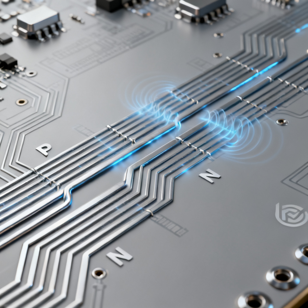
Skew, in the context of a differential pair, is the time delay mismatch between the P and N signals arriving at the receiver. This mismatch is caused by differences in the electrical length of the two traces. While the physical length is often the primary concern, skew is ultimately a function of two factors:
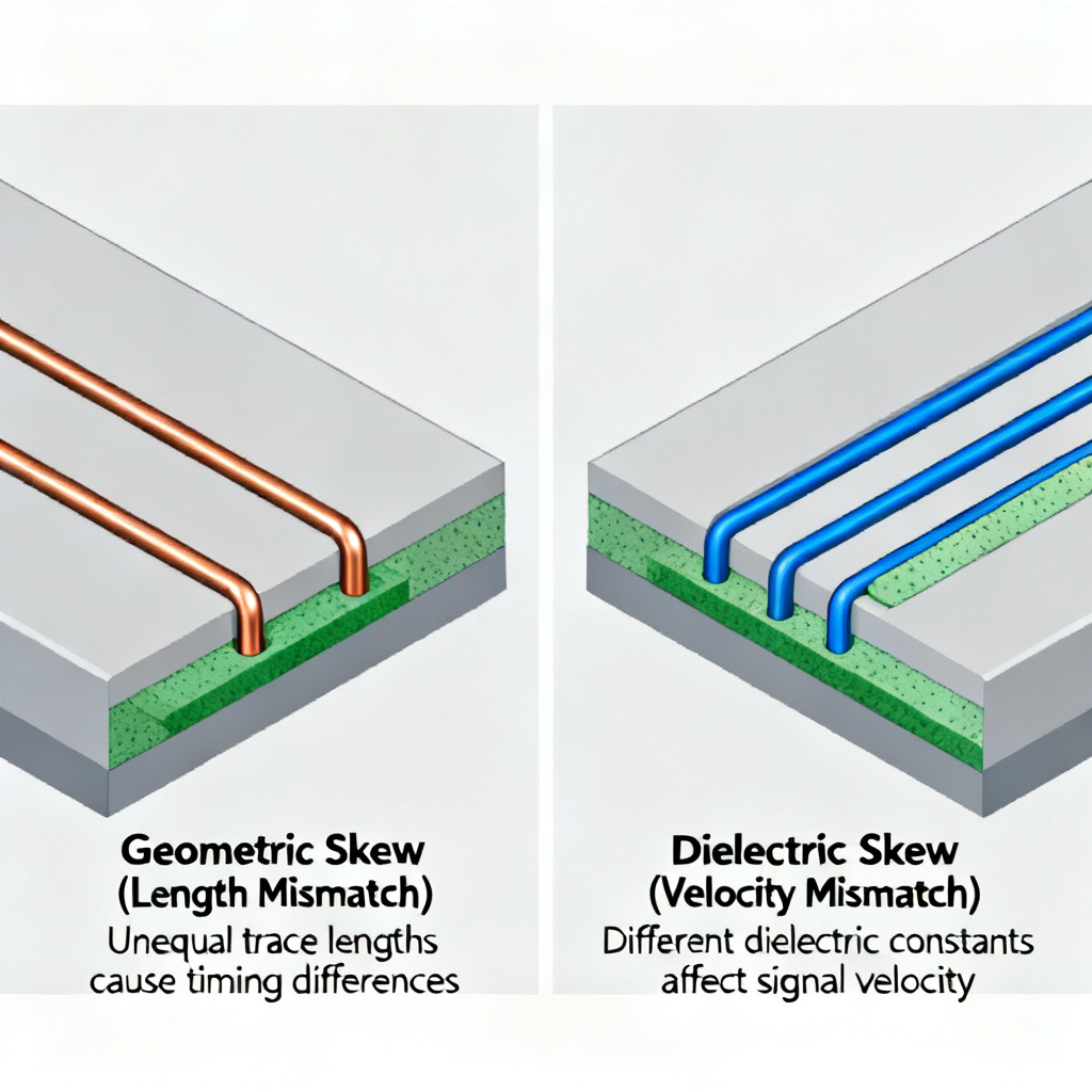
- Length Mismatch (Geometric Skew): The P and N traces have different physical lengths due to routing bends, meanders, or obstacles.
- Velocity Mismatch (Dielectric Skew): The signal propagation velocity differs between the P and N traces. This occurs when the traces are on different layers with different dielectric constants (Dk), or when the copper surface roughness or glass weave style affects the effective Dk differently for each trace.
The Core Principle: A differential signal is only truly “differential” when the two signals are perfectly opposite (180 degrees out of phase) and equal in amplitude. Skew introduces a phase shift, destroying this perfect anti-phase relationship.
Section 2: How Skew Degrades Differential Impedance
This is a nuance often misunderstood. Many engineers think impedance is purely a function of trace width, spacing, and dielectric height. While this is true for an ideal pair, skew introduces a dynamic impedance change.
2.1 The Mechanism: Mode Conversion
A differential pair supports two propagation modes:
- Differential Mode (Odd Mode): The desired mode where signals on P and N are equal and opposite. The impedance seen by each trace in this mode is the odd-mode impedance (Zodd). The differential impedance (Zdiff) is 2 * Zodd.
- Common Mode (Even Mode): An unwanted mode where signals on P and N are equal and in phase. The impedance seen by each trace is the even-mode impedance (Zeven). Zeven is always higher than Zodd because the electric field lines are pushed away from each other.
Skew causes mode conversion. When a perfect differential signal encounters a section where one trace is longer (skewed), the signal is no longer purely odd-mode. A portion of the differential energy is converted into common-mode energy. The receiver sees a mix of both modes.
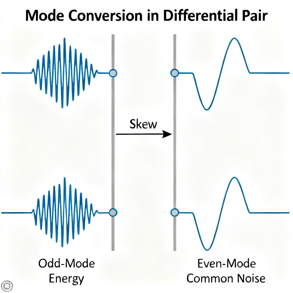
2.2 The Result: A Transient Impedance Discontinuity
Because the signal is now a mixture of odd and even modes, the effective impedance the signal “sees” at the point of the skew is no longer the designed Zdiff. It becomes a weighted average between Zdiff and Zcommon. Since Zeven is higher than Zodd, the overall impedance at the skew point increases.
- Impact: This creates a localized impedance bump. This bump causes a reflection. The reflected energy travels back to the driver, and the transmitted signal experiences ringing and distortion.
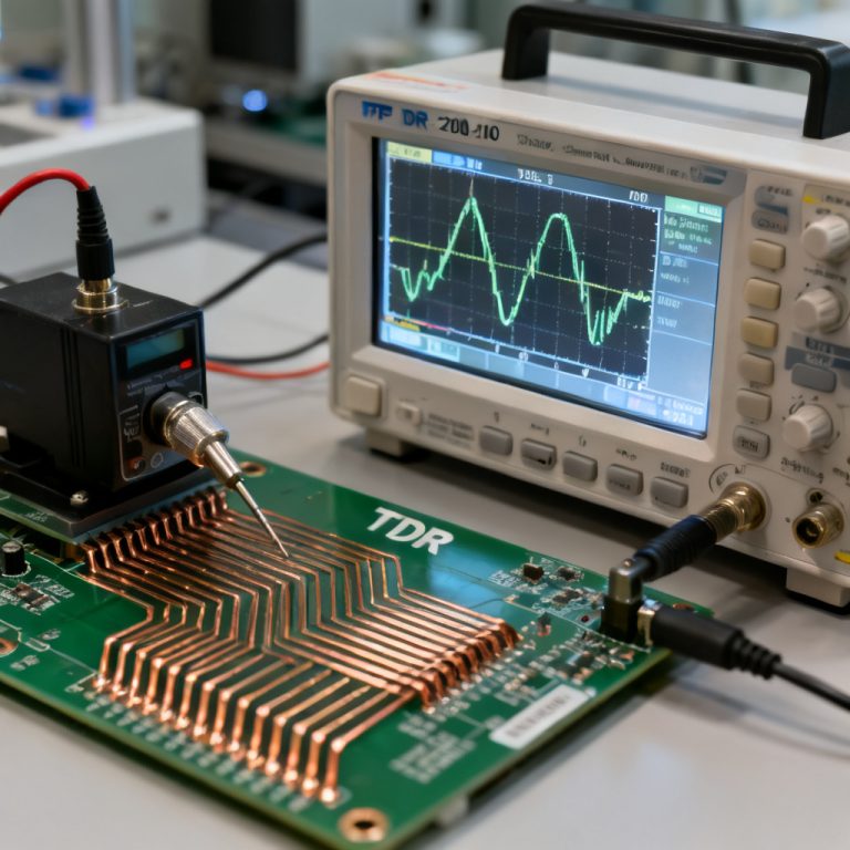
- Measurement Reality: When measured with a Time Domain Reflectometer (TDR), a skew-induced impedance discontinuity appears as a spike or dip at the location of the mismatch. It is a transient event, not a constant impedance change. The base impedance of the traces (if measured in isolation) might be correct, but the dynamic impedance during signal propagation is wrong.
Section 3: How Skew Generates Common Mode Noise (EMI)
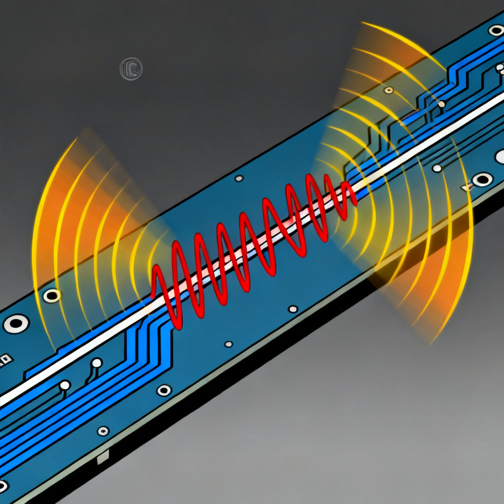
Complying with differential pair routing rules helps mitigate this most critical and well-documented consequence of skew. Common mode noise is the primary source of EMI in high-speed systems.
3.1 The Mechanism: Phase Shift Creates an Unbalanced Field
In a perfectly balanced differential pair, the equal and opposite currents (I+ and I-) generate equal and opposite magnetic fields. These fields cancel each other out in the far field, resulting in very low EMI.
When skew is present:
- Phase Shift: The P signal arrives at a given point on the line at a different time than the N signal. They are no longer 180 degrees out of phase.
- Incomplete Cancellation: Because the signals are not perfectly opposite, their magnetic fields do not completely cancel. The residual, uncanceled field radiates as EMI.
- Net Current Flow: In a perfect pair, the net current (I+ + I-) is zero. With skew, the net current is non-zero. This net current is exactly the definition of a common-mode signal.
3.2 The Quantitative Relationship: Skew vs. Common Mode Voltage
The amount of common mode voltage (Vcm) generated is directly proportional to the skew. A common rule of thumb used in industry is:
- For every 1 ps of skew, you can expect approximately 1 mV of common mode noise. (This is a rough estimate; the exact value depends on the signal rise time and amplitude).
The mathematical relationship is defined by the rise time of the signal (Tr). A fast rise time (e.g., 50 ps) is much more sensitive to skew than a slow rise time (e.g., 500 ps).
- The Critical Threshold: A widely accepted design guideline is to keep skew below 10% of the signal’s rise time (Tr).
- Example: For a signal with a 100 ps rise time, the maximum allowable skew is 10 ps.
- Example: For a signal with a 500 ps rise time, the maximum allowable skew is 50 ps.
3.3 The Impact on the Receiver
The receiver is designed to amplify the differential signal (Vdiff = Vp – Vn) and reject the common mode signal (Vcm = (Vp + Vn)/2). However, real receivers have a finite Common Mode Rejection Ratio (CMRR). If the common mode voltage generated by skew exceeds the receiver’s CMRR, the receiver will:
- Incorrectly interpret logic levels: The differential signal’s amplitude is reduced, and the common mode voltage shifts the switching threshold.
- Cause bit errors: The receiver cannot distinguish between the desired differential signal and the unwanted common mode noise.
- Saturate the input amplifier: In extreme cases, the common mode voltage can saturate the receiver’s front-end amplifier, completely blocking the signal.
Section 4: The Manufacturing Reality – Why Skew Happens in Your PCB
As a B2B PCB manufacturer, we must address the real-world causes of skew that occur during fabrication, not just in the layout.
4.1 Etching Tolerances and Impedance Control
- Uneven Etching: If the etching process is not perfectly controlled, the width of the P trace may differ from the N trace. While this primarily affects single-ended impedance, it also changes the coupling between the pair. A wider trace has higher capacitance to ground, changing its propagation velocity. This introduces a velocity mismatch (dielectric skew).
- Fiber Weave Effect: This is a major source of skew in high-speed designs. The glass weave in the core or prepreg has a higher Dk (around 6) than the epoxy resin (around 3.5). If one trace runs directly over a glass bundle and the other runs over the resin, the effective Dk for each trace is different. This causes a significant velocity mismatch. This is a pure dielectric skew and is invisible to length-matching.
4.2 Layer Stackup and Copper Roughness
- Different Layers: If the P and N traces are on different layers (e.g., Layer 2 and Layer 3), they will have different distances to the nearest reference plane. This changes their characteristic impedance and propagation velocity.
- Copper Roughness: The surface roughness of the copper foil slows down the signal. If the P and N traces are on layers with different copper foil types (e.g., standard vs. reverse treated), the velocity mismatch can be significant.
Section 5: Design and Manufacturing Strategies to Minimize Skew
5.1 Layout Rules (The Designer’s Responsibility)
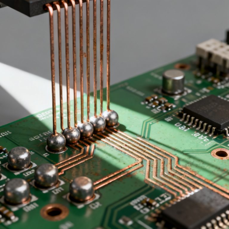
- Exact Length Matching: The most obvious rule. Use serpentine routing (trombone bends) to match lengths. However, avoid sharp 90-degree bends; use 45-degree or curved bends to minimize impedance discontinuities.
- Avoid Layer Changes: Keep the entire differential pair on the same layer. If a layer change is unavoidable, use a pair of vias (one for P, one for N) placed symmetrically.
- Glass Weave Mitigation:
- Route the pair at a 10-degree or 45-degree angle to the glass weave.
- Use “spread glass” or “open glass” laminates.
- Use a trace width that is wider than the glass bundle pitch.
- Maintain Constant Spacing: The coupling between P and N is critical. Do not change the spacing between them unless you are at a connector or IC pad. Any change in spacing changes the odd-mode impedance.
5.2 Manufacturing Tolerances (Our Commitment as Your Manufacturer)
As a high-speed PCB manufacturer, we control skew through:
- Advanced Etching Control: We use real-time etching monitoring to ensure trace width tolerances are within ±10% (and tighter for critical high-speed layers).
- Controlled Dielectric Materials: We offer a selection of low-loss, low-Dk variation materials (e.g., Rogers, Isola, or Megtron) that minimize fiber weave effects.
- Impedance Coupon Testing: We include impedance test coupons on every panel. We measure the TDR impedance of the differential pair, including the skew-induced impedance bump.
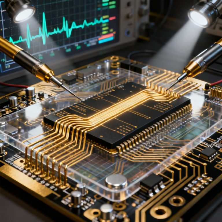
- Skew Measurement: For the most critical designs (e.g., 25+ Gbps), we can perform direct skew measurement using a Vector Network Analyzer (VNA) or a high-bandwidth oscilloscope.
| Parameter | Specification | Impact on Skew and Differential Pair Impedance |
|---|---|---|
| Trace Width Tolerance | ±10% | Uneven widths cause velocity mismatch, increasing skew and common mode noise. |
| Dielectric Constant (Dk) Variation | ±0.05 (for high-speed materials) | Dk mismatch between P and N traces leads to dielectric skew, degrading differential impedance. |
| Maximum Allowable Skew | <10% of signal rise time (Tr) | Exceeding this threshold generates common mode noise that can saturate receiver CMRR. |
| Layer-to-Layer Registration | ±0.075 mm | Misalignment between layers with P and N traces increases geometric skew. |
FAQ: How Skew Between P and N Affects Differential Pair Impedance and Common Mode Noise
What is skew between P and N in a differential pair?
Skew between P and N refers to the time delay mismatch between the positive and negative signals in a differential pair. This mismatch can be caused by differences in trace length (geometric skew) or differences in signal propagation velocity (dielectric skew).
How does skew affect differential pair impedance?
Skew causes mode conversion, where a portion of the differential signal is converted into common mode energy. This results in a transient impedance discontinuity, increasing the effective impedance at the skew point and causing signal reflections.
How does skew generate common mode noise?
Skew introduces a phase shift between the P and N signals, preventing their magnetic fields from canceling completely. The residual field radiates as EMI, and the net current flow creates a common mode signal that degrades signal integrity.
What is the maximum allowable skew for high-speed designs?
A widely accepted guideline is to keep skew below 10% of the signal’s rise time (Tr). For example, a signal with a 100 ps rise time should have no more than 10 ps of skew.
How can manufacturers minimize skew in PCB production?
Manufacturers can minimize skew through advanced etching control, using low-Dk variation materials, performing impedance coupon testing, and conducting direct skew measurement with VNA or high-bandwidth oscilloscopes for critical designs.